Preparation method of silicon substrate GaN-based epitaxial structure and epitaxial structure

An epitaxial structure, silicon substrate technology, applied in electrical components, circuits, semiconductor devices, etc., can solve the problems of large lattice mismatch, high dislocation density of GaN materials, affecting LED luminous efficiency, etc., and achieve enhanced blocking effect. , the effect of reducing the barrier peak and reducing the valence band barrier difference

Inactive Publication Date: 2019-12-31
FOSHAN NATIONSTAR SEMICON
View PDF4 Cites 5 Cited by
  • Summary
  • Abstract
  • Description
  • Claims
  • Application Information

AI Technical Summary

Problems solved by technology

[0004] However, growing GaN materials on silicon substrates faces huge technical challenges: the lattice mismatch between GaN materials and silicon substrates is large (~17%), resulting in high internal dislocation density of GaN materials (10 9 ~10 10 cm -2 ), which will seriously affect the LED luminous efficiency

Method used


Image

  • Preparation method of silicon substrate GaN-based epitaxial structure and epitaxial structure
  • Preparation method of silicon substrate GaN-based epitaxial structure and epitaxial structure
  • Preparation method of silicon substrate GaN-based epitaxial structure and epitaxial structure

Examples


preparation example Construction

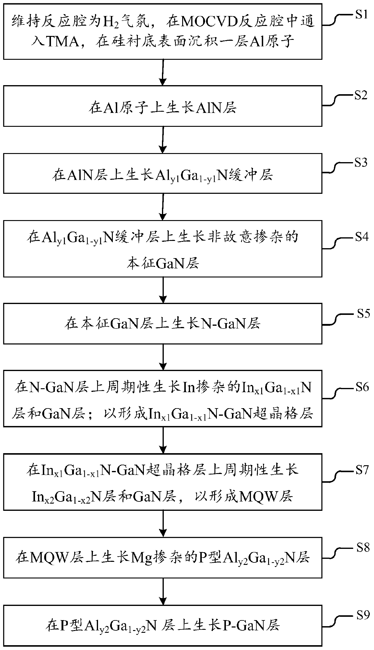
[0045] See figure 1 The present invention provides a method for preparing a GaN-based epitaxial structure on a silicon substrate, which includes the following steps:

[0046] S1: Maintain the reaction chamber as H 2 Atmosphere, pass TMA into the MOCVD reaction chamber, and deposit a layer of Al atoms on the surface of the silicon substrate;

[0047] Specifically, S1 includes:

[0048] S11: Maintain the temperature of the MOCVD reaction chamber at 1000-1100°C, the pressure at 50-200torr, and process the silicon substrate in a hydrogen atmosphere for 1 to 5 minutes;

[0049] Because there is a thin layer of SiO on the surface of the silicon substrate 2 , Using hydrogen at high temperature can remove oxygen atoms and other impurities on the surface of the substrate, laying a good foundation for the formation of a good epitaxial layer in the later stage.

[0050] S12: Maintain the temperature of the reaction chamber at 1100-1100°C and the pressure at 50-200 torr, pass trimethyl aluminum (TM...

Embodiment

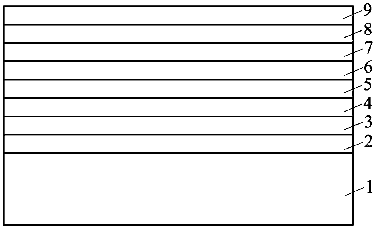
[0085] This embodiment provides a GaN-based epitaxial structure on a silicon substrate, and the preparation method thereof includes:

[0086] (1) Maintain the temperature of the MOCVD reaction chamber at 1050°C and the pressure at 150torr. 2 Process the silicon substrate for 2 minutes in an atmosphere;

[0087] (2) Maintain the temperature of the reaction chamber at 1050°C and the pressure at 150 torr, pass in TMA, and deposit a layer of Al atoms on the silicon substrate;

[0088] (3) Reduce the temperature of the reaction chamber to 980℃, the pressure to 100torr, and pass in NH 3 , TMA, grow AlN layer;

[0089] (4) Maintain the temperature of the reaction chamber at 980℃, the pressure at 100torr, and pass NH 3 , TMA and TMGa, growing Al with a thickness of 220nm y1 Ga 1-y1 N buffer layer; among them, the value of y1 ranges from 0.35 to 1; y1 decreases once with the increase of the thickness of the buffer layer;

[0090] (5) Maintain the temperature of the reaction chamber at 1080℃, the...


PUM

PropertyMeasurementUnit
thicknessaaaaaaaaaa
thicknessaaaaaaaaaa
thicknessaaaaaaaaaa

Abstract

The invention discloses a preparation method of a silicon substrate GaN-based epitaxial structure. The preparation method comprises the following steps: forming Al atoms, a AlN layer, a Aly1Ga1-y1N buffer layer, an intrinsic GaN layer, a N-GaN layer, an Inx1Ga1-x1N-GaN superlattice layer, a MQW Layer, a P-type Aly2Ga1-y2N layer and a P-GaN layer on the surface of a silicon substrate so as to obtain a finished product of the silicon substrate GaN-based epitaxial structure, wherein the value range of y2 is 0-0.3 and y2 increases with the increase of the thickness of the P-type Aly2Ga1-y2N layerin the P-type Aly2Ga1-y2N layer. The P-type Aly2Ga1-y2N layer can reduce the barrier difference between the last barrier layer and the P-type Aly2Ga1-y2N layer, i.e. the lattice mismatch between the last barrier layer and the P-type Aly2Ga1-y2N layer so as to avoid the introduction of large strain and polarization field, reduce the barrier spike formed by the valence band of the electron barrier layer and reduce the obstacle of hole injection. Meanwhile, the barrier of the conduction band of electron barrier layer increases with the increase of Al composition and the blocking effect on electron overflow quantum well is enhanced, and thus the radiation recombination efficiency of the quantum well region can be increased and the brightness of LED can be improved.

Description

Technical field [0001] The invention relates to the technical field of light emitting diodes, and in particular to a method for preparing a GaN-based epitaxial structure on a silicon substrate and an epitaxial structure. Background technique [0002] As a third-generation semiconductor material, GaN material has unique and excellent properties such as wide band gap, strong chemical bond, high temperature resistance, and corrosion resistance. Alloy semiconductors such as InGaN, GaN and AlGaN are direct bandgap semiconductors, with the band gap continuously adjustable from 0.7 to 6.2eV. They are ideal materials for the production of short-wavelength high-brightness light-emitting devices, ultraviolet detectors, and high-temperature high-frequency microelectronic devices It has been widely used in the fields of full-color large-screen displays, lighting, 5G communications and national defense. [0003] GaN-based LED lighting is rapidly replacing traditional lighting, and high-quality...

Claims


Application Information

Patent Timeline
Patent Type & Authority Applications(China)
IPC IPC(8): H01L33/00H01L33/14
CPCH01L33/0075H01L33/145
Inventor 郭嘉杰农明涛庄家铭贺卫群仇美懿
Owner FOSHAN NATIONSTAR SEMICON
Why Eureka
Try Eureka