GaN-based light-emitting diode epitaxial wafer, preparation method thereof and light-emitting diode

A technology of light-emitting diodes and epitaxial wafers, applied in the field of light-emitting diodes and GaN-based light-emitting diodes, can solve problems such as large lattice mismatch and energy band changes, unfavorable holes, and affect luminous efficiency, etc., to reduce barrier peaks, Reduces obstruction and improves lattice matching

Pending Publication Date: 2022-07-08
JIANGXI ZHAO CHI SEMICON CO LTD
View PDF0 Cites 9 Cited by
  • Summary
  • Abstract
  • Description
  • Claims
  • Application Information

AI Technical Summary

Problems solved by technology

The traditional last quantum barrier layer is the same repeated GaN layer as the previous quantum barrier layer, which will produce a large lattice mismatch and energy band change with the EBL electron blocking layer, and the sudden change of the energy band will occur in the last quantum barrier layer. A barrier peak is partially formed, which is not conducive to the injection of holes and affects the luminous efficiency

Method used


Image

  • GaN-based light-emitting diode epitaxial wafer, preparation method thereof and light-emitting diode
  • GaN-based light-emitting diode epitaxial wafer, preparation method thereof and light-emitting diode

Examples


Embodiment 1

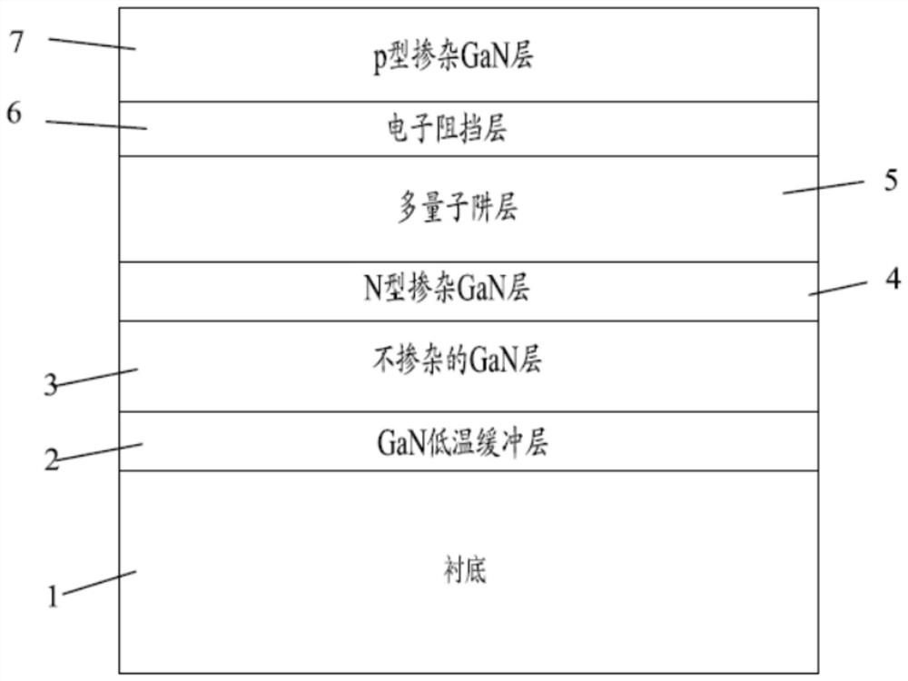
[0034] see figure 1 , shows the GaN-based light-emitting diode epitaxial wafer in the first embodiment of the present invention, including a substrate 1, and a GaN low-temperature buffer layer 2 epitaxially grown on the substrate 1 in turn, an undoped GaN layer 3, and an N-type doped GaN layer. Hetero GaN layer 4 , multiple quantum well layer 5 , electron blocking layer 6 and p-type doped GaN layer 7 .

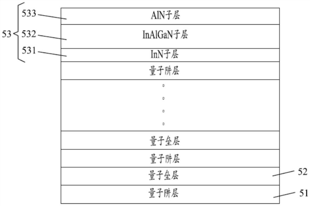
[0035] Among them, such as figure 2 As shown, the multiple quantum well layer 5 is a periodic structure in which a quantum well layer 51 and a quantum barrier layer 52 are alternately grown, and the quantum well layer 51 may be an InGaN quantum well layer specifically, and other quantum barrier layers except the last grown quantum barrier layer The layer 52 may specifically be a GaN quantum barrier layer or an InAlGaN quantum barrier layer. In this embodiment, the last grown quantum barrier layer is specifically a composite quantum barrier layer 53 , and the composite quant...

Embodiment 2

[0040] The second embodiment of the present invention provides a method for preparing a GaN-based light-emitting diode epitaxial wafer, which is used to prepare the GaN-based light-emitting diode epitaxial wafer in the first embodiment. The method specifically includes steps S21 to S28, wherein:

[0041] Step S21, providing a substrate required for epitaxial growth, preferably a sapphire substrate.

[0042] Specifically, the temperature of the reaction chamber is controlled to be 1050-1200° C., the substrate is subjected to high-temperature treatment for about 3-6 minutes in a hydrogen atmosphere, and the substrate sheet is cleaned at high temperature to reduce impurities.

[0043] In step S22, a GaN low temperature buffer layer is grown on the sapphire substrate, the growth temperature is 500°C to 700°C, and the growth pressure is 200 to 400 Torr.

[0044] Exemplarily, the growth thickness of the GaN low temperature buffer layer may be 10-30 nm.

[0045] Step S23 , growing a...

Embodiment 3

[0058] The third embodiment of the present invention provides a light-emitting diode, including the GaN-based light-emitting diode epitaxial wafer in the above-mentioned first embodiment, and the GaN-based light-emitting diode epitaxial wafer can be prepared by the preparation method of the GaN-based light-emitting diode epitaxial wafer in the above-mentioned second embodiment. Epitaxial growth is obtained.


PUM

PropertyMeasurementUnit
thicknessaaaaaaaaaa
thicknessaaaaaaaaaa
thicknessaaaaaaaaaa

Abstract

The invention provides a GaN-based light-emitting diode epitaxial wafer and a preparation method thereof, and a light-emitting diode, the GaN-based light-emitting diode epitaxial wafer comprises a multi-quantum well layer, and the multi-quantum well layer is a periodic structure formed by alternately growing quantum well layers and quantum barrier layers; wherein the last growing quantum barrier layer is a composite quantum barrier layer, the composite quantum barrier layer comprises an InN sub-layer, an InAlGaN sub-layer and an AlN sub-layer which grow in sequence, the In component of the InAlGaN sub-layer is gradually reduced in the epitaxial growth direction, and the Al component of the InAlGaN sub-layer is gradually increased in the epitaxial growth direction. The last quantum barrier is specially designed, so that lattice matching and energy level gradual transition of the quantum well layer and the P layer are improved, barrier peaks formed by valence bands of the quantum well and the electron blocking layer are effectively reduced, hole injection is facilitated, meanwhile, the effect of a part of the electron blocking layer is achieved, electron overflow is reduced, and the performance of the device is improved. The light-emitting efficiency of the light-emitting diode is improved, and the antistatic capability of the light-emitting diode is improved.

Description

technical field [0001] The invention relates to the technical field of GaN-based light-emitting diodes, in particular to a GaN-based light-emitting diode epitaxial wafer, a preparation method thereof, and a light-emitting diode. Background technique [0002] At present, GaN-based light-emitting diodes (Light Emitting Diode, LED for short) have been widely used in the field of solid-state lighting and display due to its advantages of high efficiency, energy saving, and environmental protection. As the core region of GaN-based light-emitting diodes, the multiple quantum well structure has also been widely studied. [0003] Among them, the multiple quantum well structure is generally formed by alternately stacking InGaN quantum well layers and GaN quantum barrier layers. The traditional last quantum barrier layer is the same repeating GaN layer as the previous quantum barrier layer, which will produce a large lattice mismatch and energy band change with the EBL electron blocki...

Claims


Application Information

Patent Timeline
Patent Type & Authority Applications(China)
IPC IPC(8): H01L33/06C30B25/16C30B25/18C30B29/40H01L33/00H01L33/14H01L33/32
CPCH01L33/06H01L33/145H01L33/0087H01L33/325C30B29/406C30B29/403C30B25/16C30B25/186
Inventor 张彩霞印从飞程金连胡加辉金从龙
Owner JIANGXI ZHAO CHI SEMICON CO LTD
Why Eureka
Try Eureka