Amplifier chip packaging structure and manufacturing method thereof
A chip packaging structure and amplifier technology, applied in semiconductor/solid-state device manufacturing, electric solid-state devices, semiconductor devices, etc., can solve problems such as poor performance and excessive loss of millimeter-wave amplifiers, reduce parasitic inductance, and improve production efficiency , Increase the effect of cooling efficiency
- Summary
- Abstract
- Description
- Claims
- Application Information
AI Technical Summary
Problems solved by technology
Method used
Image

Examples
Embodiment Construction
[0030] In order to make the technical problems, technical solutions and beneficial effects to be solved by the present invention clearer, the present invention will be further described in detail below in conjunction with the accompanying drawings and embodiments. It should be understood that the specific embodiments described here are only used to explain the present invention, not to limit the present invention.
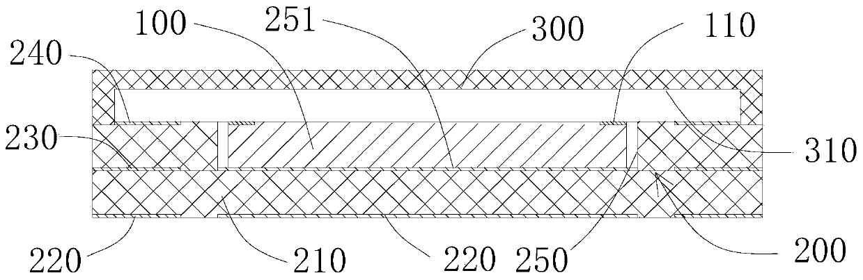
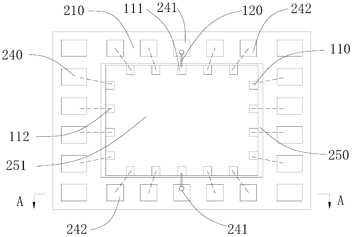
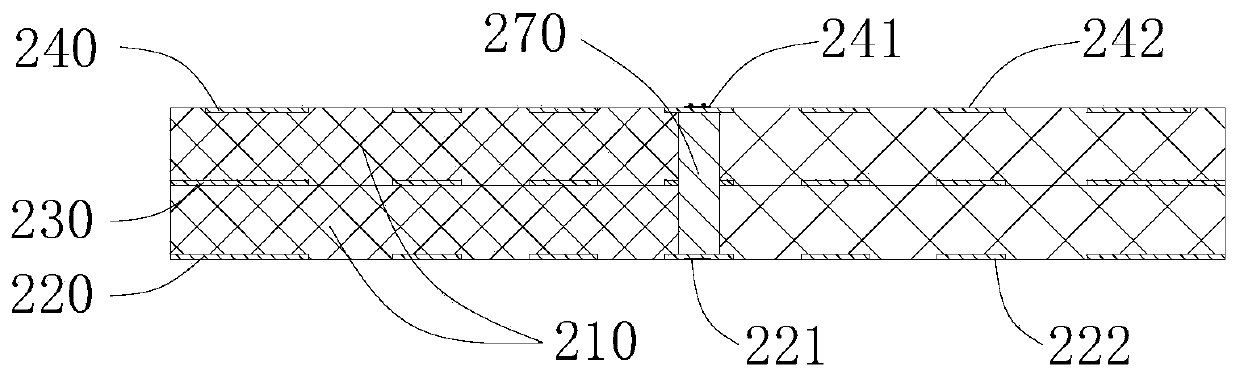
[0031] Please also refer to Figure 1 to Figure 5 , the amplifier chip package structure provided by the present invention and the method for manufacturing the package structure will now be described. The amplifier chip packaging structure includes a chip 100, a packaging substrate 200 and a cover 300; the outer periphery of the upper surface of the chip 100 is provided with several metal pressure points 110, wherein at least two metal pressure points 110 are chip radio frequency ports 111; the packaging substrate 200 is provided with There are at least two dielec...
PUM
 Abstract
Description
Claims
Application Information
 - Generate Ideas
- Intellectual Property
- Life Sciences
- Materials
- Tech Scout
- Unparalleled Data Quality
- Higher Quality Content
- 60% Fewer Hallucinations
Browse by: Latest US Patents, China's latest patents, Technical Efficacy Thesaurus, Application Domain, Technology Topic, Popular Technical Reports.
© 2025 PatSnap. All rights reserved.Legal|Privacy policy|Modern Slavery Act Transparency Statement|Sitemap|About US| Contact US: help@patsnap.com