
A method and application for monitoring the effect of defects on exciton transport in few-layer two-dimensional materials

A technology of two-dimensional materials and excitons, which is applied in the direction of material excitation analysis, optical testing of defects/defects, and analysis of materials, can solve the problem of few direct imaging measurements of exciton diffusion, and achieve the effect of optimizing the performance of components

Active Publication Date: 2021-03-30
TSINGHUA UNIV
View PDF1 Cites 0 Cited by
  • Summary
  • Abstract
  • Description
  • Claims
  • Application Information

AI Technical Summary

Problems solved by technology

But so far, direct imaging measurements of defect-influenced exciton diffusion have been scarce.
Therefore, a complete understanding of the interplay between defects and exciton transport in 2D TMDCs with defects remains challenging.

Method used


Image

  • A method and application for monitoring the effect of defects on exciton transport in few-layer two-dimensional materials
  • A method and application for monitoring the effect of defects on exciton transport in few-layer two-dimensional materials
  • A method and application for monitoring the effect of defects on exciton transport in few-layer two-dimensional materials

Examples


Embodiment Construction

[0027] In order to further understand the present invention, the methods and effects of the present invention will be further described in detail below in conjunction with specific examples. These examples are only typical descriptions of the present invention, but the present invention is not limited thereto.

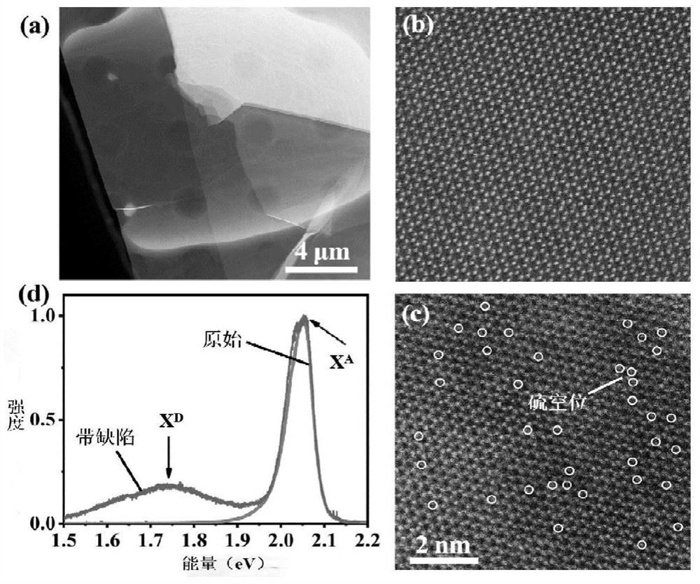
[0028]figure 1 a shows few-layer WS mechanically exfoliated from bulk crystals on a fractal-porous carbon grid or on a glass substrate. 2 flakes, the sample was characterized by optical contrast, Raman spectroscopy, and atomic force microscopy. figure 1 b is the original few-layer WS shown by atomically resolved scanning transmission electron microscopy (STEM) 2 A picture of the sample's defect-free lattice structure. Then, the pristine few-layer WS was 2 The samples were treated for 10 s to introduce defects. In WS with the defect 2 Many sulfur vacancies are observed in figure 1 Marked by a white circle in c.

[0029] Raw few-layer WS 2 and few-layer WS with f...


PUM

PropertyMeasurementUnit
wavelengthaaaaaaaaaa

Abstract

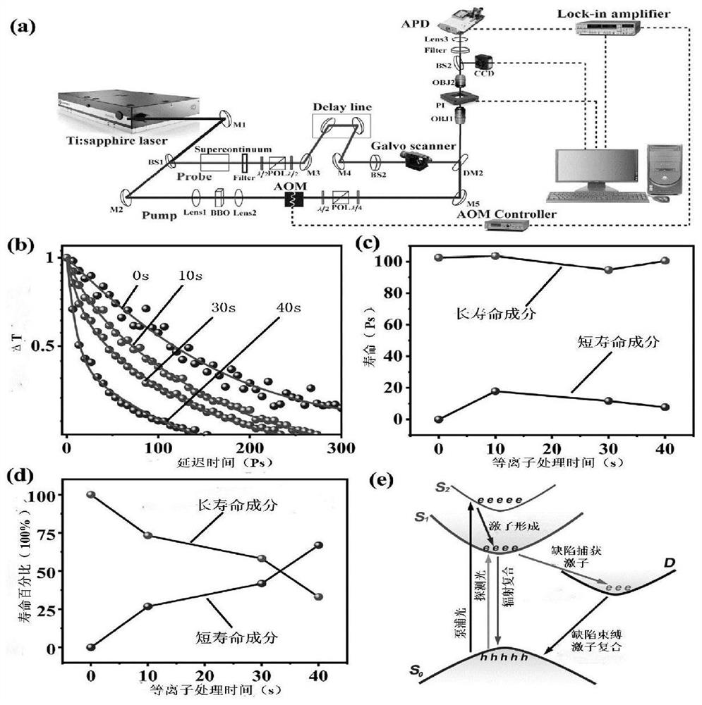
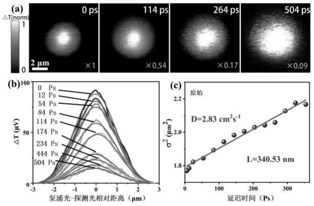
The invention relates to a method and application for monitoring the influence of defects in a few-layer two-dimensional material on exciton transmission. The method includes: providing an original few-layer two-dimensional material sample; measuring the sample through a transient absorption microscope (TAM) to obtain excitons Lifetime; TAM obtains representative TAM images of exciton densities with different delay times, and determines the diffusion coefficient and diffusion distance of excitons by Gaussian function fitting; the sample is treated with plasma and defects are identified, and then the sample is processed by TAM For measurement, use a double exponential function to fit the transient absorption kinetic curve of the sample to obtain the exciton lifetime; also determine the diffusion coefficient and diffusion distance of the excitons in the sample after plasma treatment by fitting the Gaussian function. The invention monitors the change of exciton transmission of samples under different plasma treatment times through TAM imaging, can quickly and intuitively measure the influence of defects on exciton transmission, and provides guidance for optimizing the performance of related components.

Description

technical field [0001] The invention relates to the technical field of exciton transport dynamics of nanomaterials, in particular to a method and application for monitoring the influence of defects in few-layer two-dimensional materials on exciton transport. Background technique [0002] Pristine two-dimensional transition metal dichalcogenides (TMDCs) have been widely used in various nanoscale optoelectronic components, including light-emitting diodes, excitonic transistors, and photovoltaic applications. Nanoscale energy transport in the form of excitons is at the heart of these TMDC-based devices. For example, in light-gathering applications, excitons are generated by photoexcitation and must then move efficiently to the interface where the exciton dissociates to generate photovoltage or photocurrent. However, in existing components, defects are always introduced during the prefabrication and nanofabrication of 2D TMDCs. Defects affect the band structure, crystal struct...

Claims


Application Information

Patent Timeline
Patent Type & Authority Patents(China)
IPC IPC(8): G01N21/63G01N21/88G01N21/95G01N23/04G01N23/20
CPCG01N21/63G01N21/636G01N21/8851G01N21/95G01N23/04G01N23/20G01N2021/637G01N2223/102G01N2223/418G01N2223/646
Inventor 刘大猛刘欢王冲陈新春李津津雒建斌
Owner TSINGHUA UNIV
Learn More