Method for direct growth of SOI

A direct and epitaxial growth technology, applied in the field of microelectronics, can solve the problems of complex preparation process and high production cost, and achieve the effects of simplifying the preparation process, saving consumables, and reducing production costs

Pending Publication Date: 2020-01-31
SHENYANG SILICON TECH
View PDF0 Cites 0 Cited by
  • Summary
  • Abstract
  • Description
  • Claims
  • Application Information

AI Technical Summary

Problems solved by technology

[0004] At present, bonding technology is usually used to prepare SOI, and thin-film SOI usually adopts implantation and other processes. There are problems such as complex preparation process and high production cost, which need to be improved urgently.

Method used


Image

  • Method for direct growth of SOI
  • Method for direct growth of SOI
  • Method for direct growth of SOI

Examples


Embodiment 1

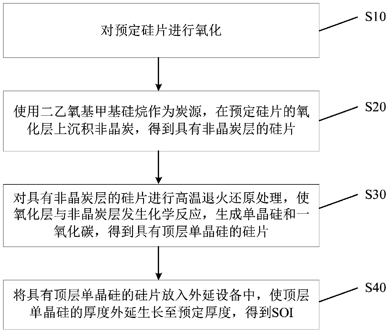
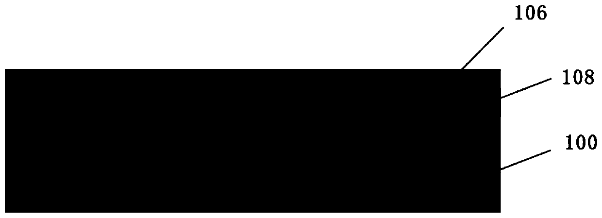
[0025] refer to Figure 1 to Figure 4 , in step S10, the predetermined silicon wafer 100 is oxidized.

[0026] Preferably, the predetermined silicon wafer 100 is a P-type silicon wafer with a resistivity of 8.5-11.5 ohm.cm and a crystal orientation.

[0027] As an example, dry oxygen and / or wet oxygen oxidation may be used to oxidize the predetermined silicon wafer 100 .

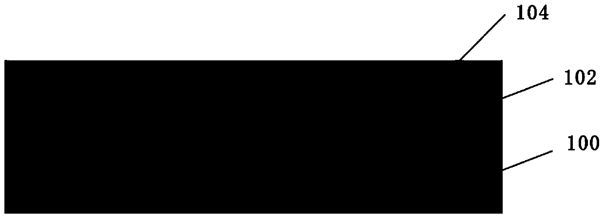
[0028] Preferably, the predetermined silicon wafer 100 is oxidized under the oxidation conditions of an oxygen flow rate of 500 sccm, an air pressure of 230 torr, and a temperature of 900° C. to obtain a silicon wafer with an oxide layer 102 having a thickness of 1 μm.

[0029] In step S20, use diethoxymethylsilane (DEMS) as a carbon source (i.e., C source), deposit amorphous carbon on the oxide layer 102 of the predetermined silicon wafer 100, and obtain a silicon wafer with an amorphous carbon layer 104 .

[0030] Preferably, under the deposition conditions that the flow rate of the carbon source is 1....

Embodiment 2

[0049] This embodiment provides a method for directly growing SOI, including:

[0050] Under the oxidation conditions of an oxygen flow rate of 900 sccm, an air pressure of 460 torr, and a temperature of 950° C., the predetermined silicon wafer 100 is oxidized to obtain a silicon wafer with an oxide layer 102 having a thickness of 1 μm.

[0051] Under the deposition conditions that the flow rate of the carbon source is 4.5g / s and the deposition temperature is 550°C, the chemical vapor deposition method is used to deposit amorphous carbon on the oxide layer 102 of the predetermined silicon wafer 100 to obtain the thickness of the amorphous carbon layer 104 70A silicon wafer.

[0052] Put the silicon wafer with the amorphous carbon layer 104 into a high-temperature furnace, under the conditions of high-temperature annealing reduction treatment with an annealing pressure of 0.8 torr, an annealing temperature of 1300° C., and an annealing time of 6 hours, with helium as protection...

Embodiment 3

[0056] This embodiment provides a method for directly growing SOI, including:

[0057] The predetermined silicon wafer 100 is oxidized under the oxidation conditions of an oxygen flow rate of 1900 sccm, a gas pressure of 760 torr, and a temperature of 1000° C. to obtain a silicon wafer with an oxide layer 102 having a thickness of 1 μm.

[0058] Under the deposition conditions that the flow rate of the carbon source is 3g / s and the deposition temperature is 750°C, the chemical vapor deposition method is used to deposit amorphous carbon on the oxide layer 102 of the predetermined silicon wafer 100, and the thickness of the amorphous carbon layer 104 is obtained. 100A silicon wafer.

[0059] Put the silicon wafer with the amorphous carbon layer 104 into a high-temperature furnace, under the conditions of high-temperature annealing reduction treatment with an annealing pressure of 5 torr, an annealing temperature of 1400° C., and an annealing time of 6 hours, with helium as prote...


PUM

PropertyMeasurementUnit
thicknessaaaaaaaaaa
thicknessaaaaaaaaaa
evennessaaaaaaaaaa

Abstract

The invention provides a method for direct growth of SOI. The method comprises the following steps: oxidizing a predetermined silicon wafer; depositing amorphous carbon on an oxide layer of the predetermined silicon wafer by using diethoxymethylsilane as a carbon source so as to obtain a silicon wafer having an amorphous carbon layer; performing high-temperature annealing reduction treatment on the silicon wafer with the amorphous carbon layer to enable the oxide layer and the amorphous carbon layer to have chemical reaction so as to generate monocrystalline silicon and carbon monoxide and obtain the silicon wafer with the top monocrystalline silicon, wherein the treatment process is protected by inert gas; and putting the silicon wafer with the top monocrystalline silicon into epitaxial equipment and the thickness of the top monocrystalline silicon is epitaxially grown to a predetermined thickness so as to obtain the SOI. According to the method of direct growth of the SOI, the preparation process flow can be simplified, the production cost is low and the production capacity is high.

Description

technical field [0001] The invention relates to the technical field of microelectronics, in particular to a method for directly growing SOI. Background technique [0002] Silicon-On-Insulator (SOI) is a new type of silicon-based semiconductor material with a unique three-layer structure of "Si / insulator / Si". SOI technology introduces a layer of insulating buried layer (ie, buried oxide layer) between the top silicon and the back substrate, through the insulating buried layer (usually silicon dioxide SiO 2 ) realizes the full dielectric isolation of the device and the substrate. [0003] Therefore, by forming a semiconductor thin film on an insulator, silicon material makes SOI material have incomparable advantages over bulk silicon: (1) It can realize the dielectric isolation of components in integrated circuits and completely eliminate the parasitic latch effect in bulk silicon CMOS circuits (2) Integrated circuits made of SOI have the advantages of small parasitic capaci...

Claims


Application Information

Patent Timeline
Patent Type & Authority Applications(China)
IPC IPC(8): H01L21/762
CPCH01L21/7624H01L21/76294
Inventor 贾文博
Owner SHENYANG SILICON TECH
Why Eureka
Try Eureka