Integrated circuit defect image recognition and classification system based on fusion deep learning model

A deep learning and image recognition technology, which is applied in image analysis, character and pattern recognition, image enhancement, etc., can solve the problems of low efficiency of manual recognition and low recognition rate of defect image categories, so as to reduce the cost of recognition, increase the level of automation, The effect of improving the yield rate

Inactive Publication Date: 2020-02-07
上海众壹云计算科技有限公司
View PDF0 Cites 21 Cited by
  • Summary
  • Abstract
  • Description
  • Claims
  • Application Information

AI Technical Summary

Problems solved by technology

[0006] The existing wafer inspection machine has a low recognition rate of de

Method used


Image

  • Integrated circuit defect image recognition and classification system based on fusion deep learning model
  • Integrated circuit defect image recognition and classification system based on fusion deep learning model
  • Integrated circuit defect image recognition and classification system based on fusion deep learning model

Examples


Embodiment Construction

[0027] The technical solutions in the embodiments of the present invention will be clearly and completely described below in conjunction with the accompanying drawings in the embodiments of the present invention. Obviously, the described embodiments are only some of the embodiments of the present invention, not all of them. Based on the embodiments of the present invention, all other embodiments obtained by persons of ordinary skill in the art without making creative efforts belong to the protection scope of the present invention.

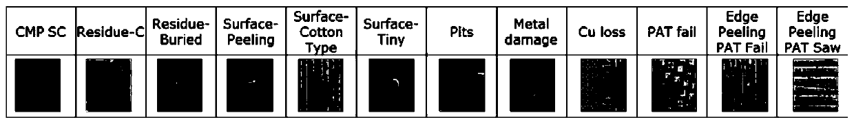
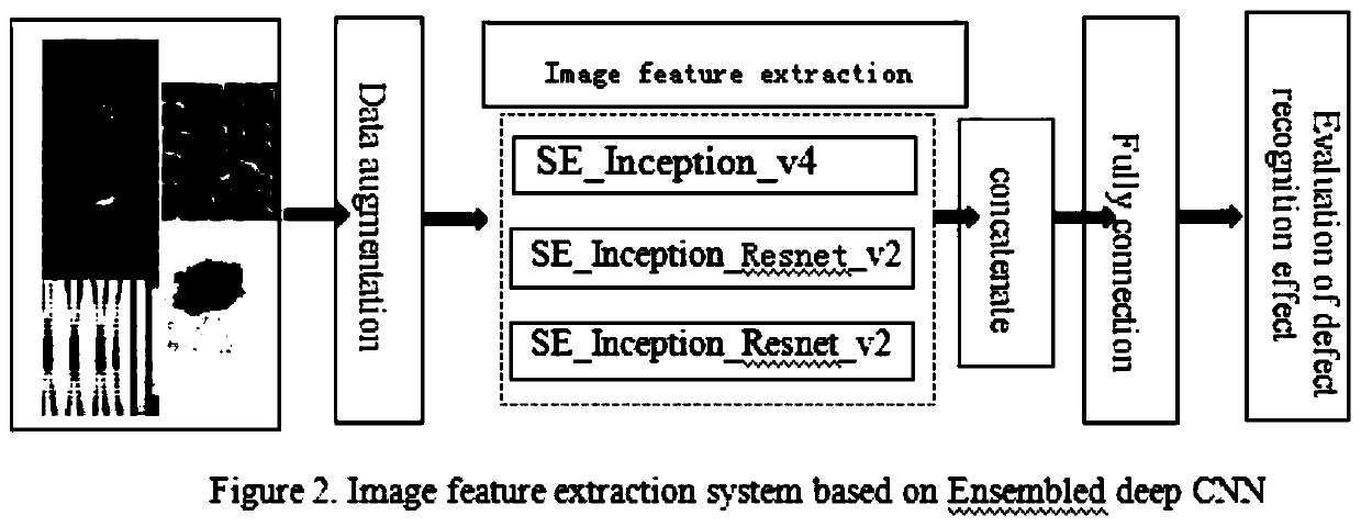
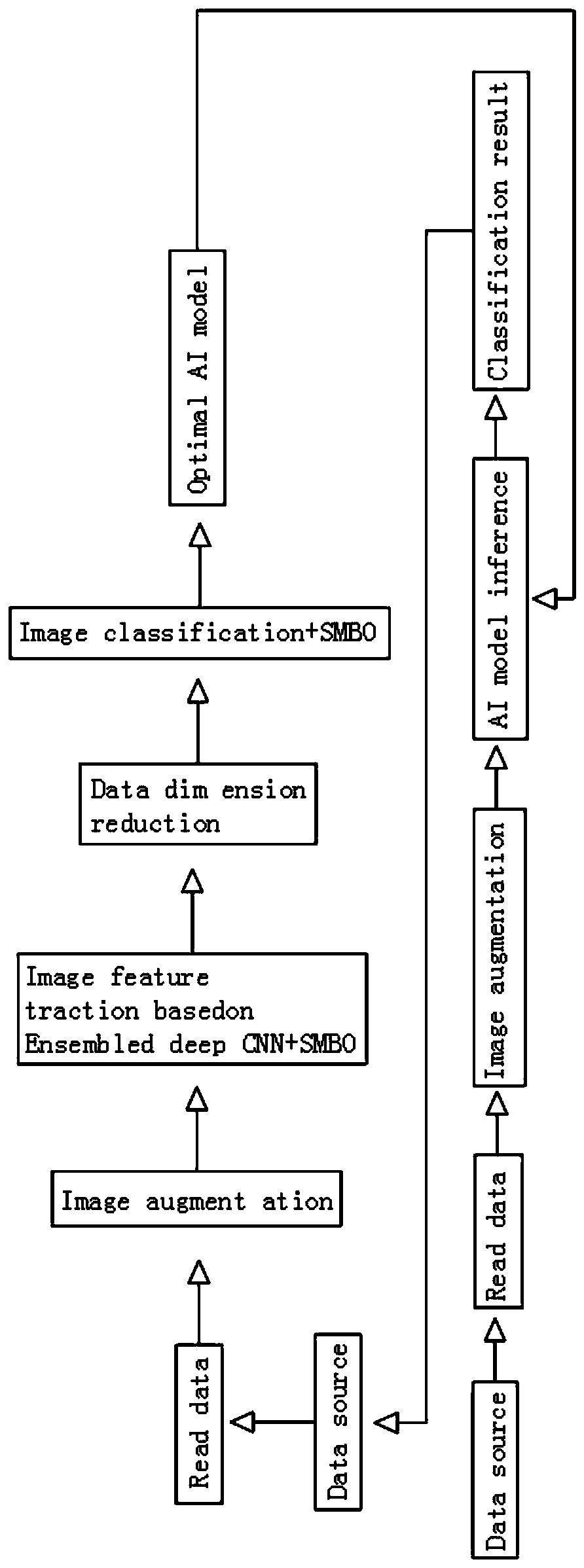
[0028] see Figure 1~3, in an embodiment of the present invention, an integrated circuit defect image recognition and classification system based on a fusion deep learning model is used as a neural network that simulates the process of processing visual images by the human brain. The convolutional network consists of a convolutional layer, a pooling layer, and a fully connected layer. composition. Among them, the convolutional layer cooperates wit...


PUM


Abstract

The invention discloses an integrated circuit defect image recognition and classification system based on a fusion deep learning model, and provides a mode of using a fusion model based on a deep convolutional neural network (CNN) to carry out on-line automatic recognition and classification on defect images of a wafer so as to timely detect the change of the number of various defects of the wafer. The core mechanism of the method is a defect image feature extraction method constructed by two deep learning models integrated into a learning mechanism. According to the deep CNN fusion model, a Combined3 defect image classification model is constructed on the basis of two frameworks of SE _ Inception _ V4 and SE _ Inception _ ResNet _ V2; and a sequence model optimization (SMBO) algorithm isutilized to perform hyper-parameter optimization on the fusion depth CNN recognition model, so that the model recognition precision is improved. Increasing automation levels. And the identification cost is reduced because an engineer is replaced by the AI model, and the working efficiency is greatly improved. Based on a real-time identification and classification result, engineers can count defectdata and search reasons in time, so that process parameters are adjusted, and the yield is improved.

Description

technical field [0001] The invention relates to the field of image recognition and classification systems, in particular to an integrated circuit defect image recognition and classification system based on a fusion deep learning model. Background technique [0002] Integrated circuit wafer manufacturing is to make circuits and electronic components (such as transistors, capacitors, logic switches, etc.) on the wafer. The processing procedures are usually related to the type of product and the technology used. Repeated steps such as meteorological precipitation, photolithography, etching, ion implantation, chemical mechanical polishing, etc., finally complete the processing and production of several layers of circuits and components on the wafer. In the semiconductor manufacturing process, in order to monitor any abnormal defect characteristics and quickly respond to process problems, it is necessary to use online measurement tools to inspect after a certain process step and ...

Claims


Application Information

Patent Timeline
IPC IPC(8): G06T7/00G06K9/62G06N3/04
CPCG06T7/0004G06T2207/20081G06T2207/30148G06N3/045G06F18/241
Inventor 林义征
Owner 上海众壹云计算科技有限公司
Why Eureka
Try Eureka