A 11t TFET SRAM Cell Circuit Structure with Low Power Consumption and High Write Margin

A unit circuit and circuit structure technology, applied in information storage, static memory, digital memory information and other directions, can solve the problems of read noise margin and static power consumption.

Active Publication Date: 2021-09-14
ANHUI UNIVERSITY
View PDF7 Cites 0 Cited by
  • Summary
  • Abstract
  • Description
  • Claims
  • Application Information

AI Technical Summary

Problems solved by technology

For NTFET, when the source voltage is higher than the drain voltage, there will always be a p-i-n forward bias current that is not controlled by the gate, which will affect its static noise margin and read noise margin when it is applied in an SRAM circuit. Accuracy and static power consumption have a severe impact on the

Method used


Image

  • A 11t TFET SRAM Cell Circuit Structure with Low Power Consumption and High Write Margin
  • A 11t TFET SRAM Cell Circuit Structure with Low Power Consumption and High Write Margin
  • A 11t TFET SRAM Cell Circuit Structure with Low Power Consumption and High Write Margin

Examples


Embodiment Construction

[0025] The technical solutions in the embodiments of the present invention will be clearly and completely described below in conjunction with the accompanying drawings in the embodiments of the present invention. Obviously, the described embodiments are only some of the embodiments of the present invention, not all of them. Based on the embodiments of the present invention, all other embodiments obtained by persons of ordinary skill in the art without making creative efforts belong to the protection scope of the present invention.

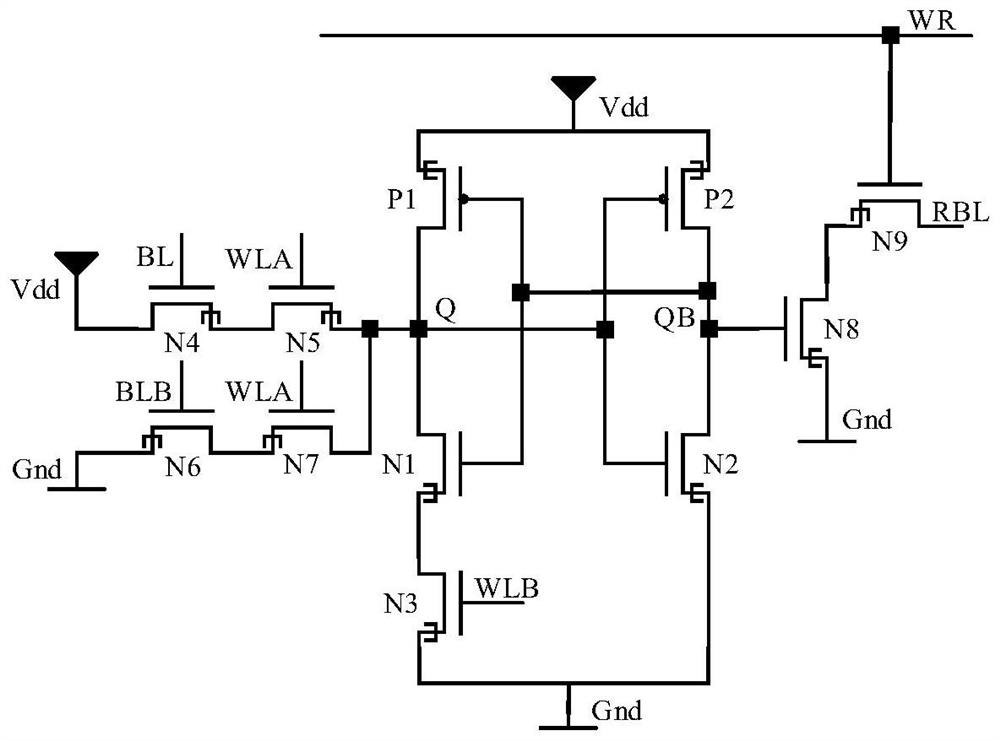
[0026] Embodiments of the present invention will be further described in detail below in conjunction with the accompanying drawings, as figure 1 Shown is the overall schematic diagram of the 11T TFET SRAM cell circuit structure with low power consumption and high write margin provided by the embodiment of the present invention. The circuit structure includes nine NTFET transistors and two PTFET transistors, and the nine NTFET transistors are sequent...


PUM


Abstract

The invention discloses a 11T TFET SRAM unit circuit structure with low power consumption and high write margin, which includes nine NTFET transistors and two PTFET transistors, the nine NTFET transistors are sequentially denoted as N1-N9, and the two PTFET transistors are denoted sequentially For P1 and P2, VDD is connected to the drain of the NTFET transistor N4, and VDD is also electrically connected to the sources of the PTFET transistor P1 and the PTFET transistor P2; the drain of the PTFET transistor P1 is connected to the drain of the NTFET transistor N1 and the NTFET transistor N5 The source of the PTFET transistor N7, the drain of the NTFET transistor N7, the gate of the PTFET transistor P2, and the gate of the NTFET transistor N2 are electrically connected. The circuit structure not only solves the problem of poor structure retention and read ability of the traditional TFET SRAM unit, but also improves the stability of the SRAM unit.

Description

technical field [0001] The invention relates to the technical field of integrated circuits, in particular to a 11T TFETSRAM unit circuit structure with low power consumption and high write margin. Background technique [0002] With the continuous improvement of MOS manufacturing process, the device size is also reduced, which promotes the vigorous development and technological progress of the integrated circuit industry. However, MOSFET (Metal-Oxide Semiconductor Field Effect Transistor) is an important part of digital integrated circuits and analog integrated circuits. Due to the continuous reduction of its feature size, the threshold voltage gradually increases, and the off-state current deteriorates day by day, making the static leakage current of the circuit And static power consumption is seriously increased, so people's demand for low-power devices is increasingly urgent. In addition, the sub-threshold swing of MOSFET at room temperature is limited by the thermoelectr...

Claims


Application Information

Patent Timeline
Patent Type & Authority Patents(China)
IPC IPC(8): G11C11/412G11C11/419
CPCG11C11/4125G11C11/419
Inventor 李正平陈朌盼蔺智挺彭春雨吴秀龙卢文娟陈军宁
Owner ANHUI UNIVERSITY
Why Eureka
Try Eureka