Method for representing nano film micro-area deformation area by virtue of combination of photetching technique and transmitted electron microtechnique

A technology of transmission electron microscopy and lithography technology, which is applied in the field of joint characterization of nano-film micro-region deformation by lithography technology and transmission electron microscopy technology

Active Publication Date: 2013-04-17
BEIJING UNIV OF TECH
View PDF2 Cites 20 Cited by
  • Summary
  • Abstract
  • Description
  • Claims
  • Application Information

AI Technical Summary

Problems solved by technology

[0006] Aiming at the problems existing in the prior art, the present invention provides a method for jointly characterizing the deformation of nano-film micro-regions by photolithography technology and high-resolution transmission electron microscope technology. This method develops a nano-film transfer technology that can deform nano-indentations The area is directly transferred to a high-resolution transmission electron microscope for quasi-in-situ observation. This method can make full use of the advantages of the large-angle biaxial tilting of the commercial TEM sample rod, and directly go deep into the atomic scale to study the thickness

Method used


Image

  • Method for representing nano film micro-area deformation area by virtue of combination of photetching technique and transmitted electron microtechnique
  • Method for representing nano film micro-area deformation area by virtue of combination of photetching technique and transmitted electron microtechnique
  • Method for representing nano film micro-area deformation area by virtue of combination of photetching technique and transmitted electron microtechnique

Examples


Embodiment

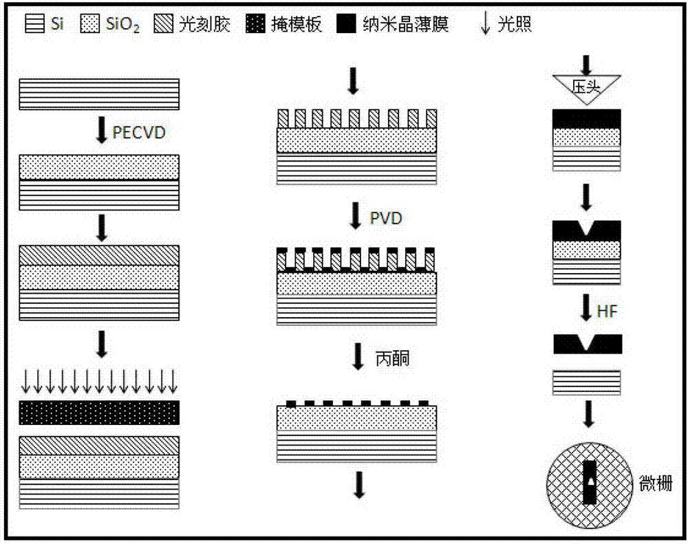
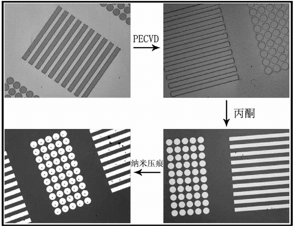
[0035] 1) Make a silicon wafer with a specific pattern

[0036] ① Prepare a circular or rectangular mask for the experiment. The diameter of the circular mask of the mask is 45 microns, and the interval is 10 microns; the width of the square mask is 35 microns, the length is 500 microns, and the interval is 30 microns. All patterns Evenly distributed on the mask plate.

[0037] ② Choose a silicon wafer in the direction, and then use plasma-enhanced chemical vapor deposition (PECVD) to prepare an amorphous silicon dioxide layer with a thickness of 200-300nm on the silicon wafer.

[0038] ③Clean the substrate. Put the substrate into the acetone solution and ultrasonically clean it for 5 minutes, then put the substrate into the alcohol solution and ultrasonically clean it for 5 minutes to remove the residual acetone, finally clean it with deionized water, and dry the sample with nitrogen.

[0039] ④ Throw away the glue on the substrate. In the glue-spinning stage, the speed t...


PUM

PropertyMeasurementUnit
Thicknessaaaaaaaaaa
Diameter sizeaaaaaaaaaa
Widthaaaaaaaaaa

Abstract

The invention provides a method for representing a nano film micro-area deformation area by virtue of combination of a photetching technique and a transmitted electron microtechnique and belongs to the field of film nanoindentation representation. The invention discloses a method for representing a 10-100 nano film microarea deformation area by virtue of combination of a photetching technique and a transmitted electron microtechnique. According to the method, an indentated film is directly transferred into a transmission electron microscope so as to be observed by virtue of a film transfer technology; the microdefect formation, interaction and evolutionary process during a nano film elastoplasticity transition process in a nanoindentation acting process is directly disclosed from the aspect of atom scale; the direct relation between microstructure and macromechanic performance is disclosed; and the method belongs to a film nanoindentation representation method.

Description

Technical field: [0001] The invention discloses a method for jointly characterizing the deformation of 10-100 nanometer film micro-regions by photolithography technology and transmission electron microscopy technology. Through the film transfer technology, the indented film is directly transferred to the transmission electron microscope for observation, and it can be observed from the atomic scale. It directly reveals the formation, interaction and evolution process of micro-defects in the elastic-plastic transition process of nano-film during nano-indentation, reveals the direct relationship between micro-structure and macro-mechanical properties, and belongs to the film nano-indentation characterization method. Background technique: [0002] The development of semiconductor devices or micro-nano electromechanical systems (MEMS) to high-density, high-speed and flexible devices requires the development of the important structural unit - metal thin film interconnection line to...

Claims


Application Information

Patent Timeline
IPC IPC(8): G01B15/06
Inventor 张跃飞李玉洁臧鹏韩晓东张泽
Owner BEIJING UNIV OF TECH
Why Eureka
Try Eureka