

Integrated preparation device of high-flux magnetron sputtering nano film device
A nano-film and preparation device technology, which is applied in the field of integrated preparation devices for high-throughput magnetron sputtering nano-film devices, can solve the problem that the amount of samples processed at one time needs to be increased, and achieve full use of space, uniform coating, and easy The effect of control
- Summary
- Abstract
- Description
- Claims
- Application Information
AI Technical Summary
Problems solved by technology
Method used
Image

Examples
Embodiment 1
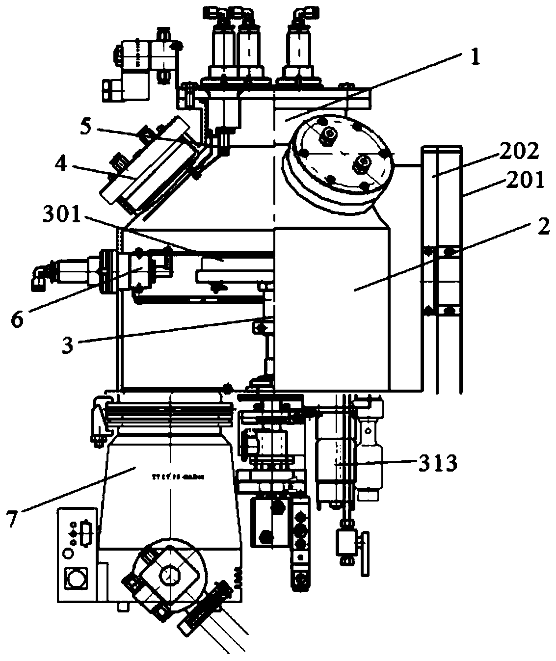
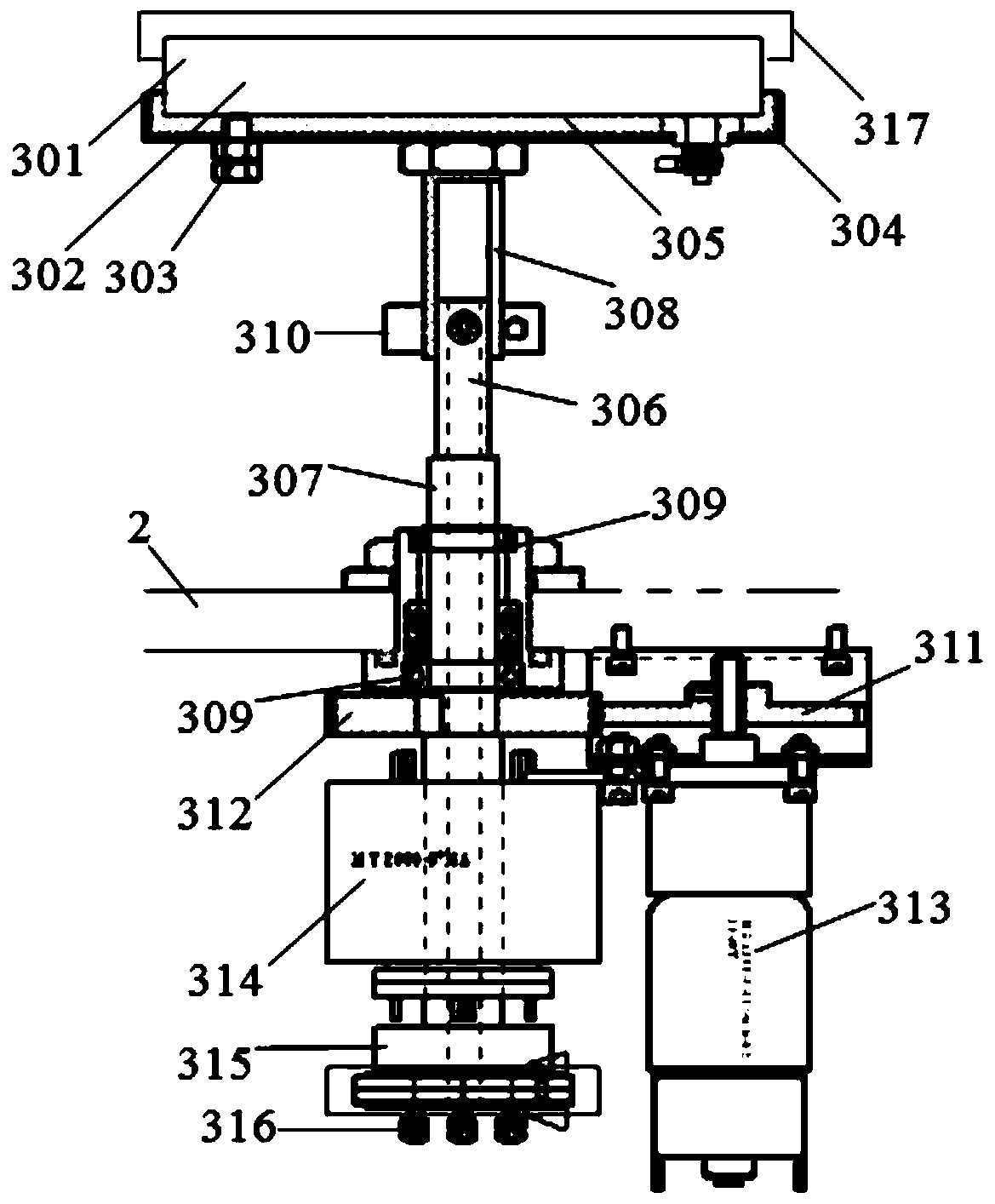
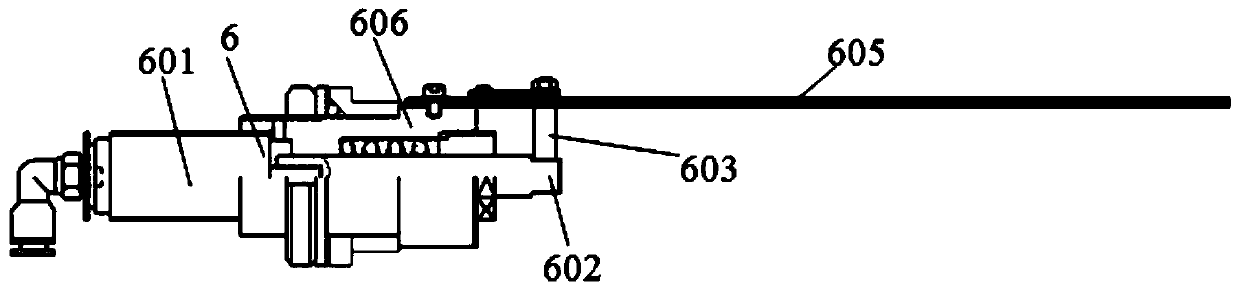
[0068] The structure of the host 1 of the high-throughput magnetron sputtering nanometer thin film device integrated preparation device in this embodiment is as follows figure 1 As shown, the host 1 includes a working chamber 2, a sample holder 3, a magnetron target 4, a target baffle 5 and a sample baffle 6, the host 1 is the core working part of the preparation device, and the magnetron sputtering coating operation is performed in the working chamber 2 internally. The upper part of the working chamber 2 is in the shape of a circular truncated table, the side of the circular table is an inclined wall surface, and the inclination angle between the inclined wall surface and the horizontal plane is 45 degrees. The middle and lower parts of the working chamber 2 are in the shape of a cylinder. One side of the working chamber 2 is provided with a sample door 201 for the entry and exit of samples, and a magnetic plate 202 is provided between the sample door 201 and the door frame ...
Embodiment 2
[0099] This embodiment uses the high-throughput magnetron sputtering nanometer thin-film device integrated preparation device of Embodiment 1. In this embodiment, 100 inorganic all-solid-state electrochromic thin-film devices are prepared. The specific method is as follows:
[0100] (1) Turn on the power supply, according to the requirements of sputtering coating, the coating time of five magnetron targets 4 is set to be 5 seconds, and five magnetron targets 4 start coating successively in clockwise order, and DC power supply, radio frequency power supply, bias The current and voltage of the piezoelectric power supply and the heating power supply, the temperature of the sample stage 301 set on the temperature controller;
[0101] (2) plastic substrate is placed on sample stage 301 by sample door 201, adjust sample stage 301 height, make whole sample stage 301 enter the coating range of magnetron target 4, close sample door 201, start vacuum pump 8 and molecular pump 7, Monitor...
PUM
| Property | Measurement | Unit |
|---|---|---|
| angle | aaaaa | aaaaa |
| diameter | aaaaa | aaaaa |
Abstract
Description
Claims
Application Information