Tin oxide-based thin film transistor based on plasma enhanced atomic layer deposition gate insulating layer and preparation method

A gate insulating layer, atomic layer deposition technology, applied in transistors, semiconductor/solid-state device manufacturing, semiconductor devices, etc., can solve the problems of low "on-state" current, low device mobility, low dielectric constant, etc. The effect of reducing the turn-on voltage, low cost, and simple preparation process

Inactive Publication Date: 2020-02-11
SOUTH CHINA UNIV OF TECH
View PDF3 Cites 2 Cited by
  • Summary
  • Abstract
  • Description
  • Claims
  • Application Information

AI Technical Summary

Problems solved by technology

Due to their low dielectric constant (approximately 3.9) and low capacitance, typically resulting in low device mobility and low "on" current

Method used


Image

  • Tin oxide-based thin film transistor based on plasma enhanced atomic layer deposition gate insulating layer and preparation method
  • Tin oxide-based thin film transistor based on plasma enhanced atomic layer deposition gate insulating layer and preparation method
  • Tin oxide-based thin film transistor based on plasma enhanced atomic layer deposition gate insulating layer and preparation method

Examples


Embodiment Construction

[0029] The present invention will be further described in detail below in conjunction with the embodiments and the accompanying drawings, but the embodiments of the present invention are not limited thereto.

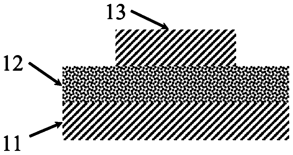
[0030] A tin oxide-based thin film transistor based on plasma-enhanced atomic layer deposition gate insulating layer, comprising: a substrate, a gate, a gate insulating layer, an active layer and a source-drain electrode arranged in sequence, wherein: the gate insulating layer The aluminum oxide film is prepared by plasma-enhanced atomic layer deposition, and the active layer is a silicon-doped tin oxide film prepared by magnetron sputtering deposition.

[0031] The invention introduces high-quality aluminum oxide as the grid insulating layer, improves the interface quality of the grid insulating layer / active layer, and effectively improves device mobility and stability. Alumina film is prepared by atomic layer deposition, the material of the gate insulating layer is alu...


PUM

PropertyMeasurementUnit
thicknessaaaaaaaaaa
thicknessaaaaaaaaaa
thicknessaaaaaaaaaa

Abstract

The invention belongs to the technical field of thin film transistors, and relates to a tin oxide-based thin film transistor based on a plasma enhanced atomic layer deposition gate insulating layer, which comprises a substrate, a gate, a gate insulating layer, an active layer, a source and a drain arranged in sequence, wherein the gate insulating layer is an aluminum oxide thin film prepared through plasma enhanced atomic layer deposition, and the active layer is a silicon-doped tin oxide thin film prepared through magnetron sputtering deposition. The tin oxide-based thin film transistor adopts a plasma enhanced atomic layer deposition method to prepare aluminum oxide with a high dielectric constant as a gate insulating layer, an amorphous silicon doped tin oxide semiconductor material isused as an active layer material, the interface defect mode of the active layer/gate insulating layer and the turn-on voltage of the device are reduced, and the mobility and the stability of the device are remarkably improved. The invention further provides a preparation method for the tin oxide-based thin film transistor based on the plasma enhanced atomic layer deposition gate insulating layer.

Description

technical field [0001] The invention belongs to the technical field of thin film transistors, and relates to a tin oxide-based thin film transistor based on plasma-enhanced atomic layer deposition gate insulating layer and a preparation method. Background technique [0002] At present, flat panel display technology is developing rapidly, and large-size, high-resolution, high-refresh rate displays have become the mainstream. Among them, the core technology of the flat panel display industry is thin-film transistor (TFT) backplane technology, and it is very important to improve the performance of TFT and reduce the production cost. In traditional TFTs, silicon oxide or silicon nitride is used as the gate insulating layer. Due to their low dielectric constant (approximately 3.9), low capacitance typically results in low device mobility and low "on" current. The insulating layer material with high dielectric constant has the advantages of high dielectric constant, relatively l...

Claims


Application Information

Patent Timeline
Patent Type & Authority Applications(China)
IPC IPC(8): H01L29/786H01L29/24H01L29/49H01L29/51H01L21/34H01L21/443
CPCH01L21/443H01L29/247H01L29/4908H01L29/517H01L29/66969H01L29/78693
Inventor 宁洪龙刘贤哲姚日晖袁炜健张旭张观广梁志豪梁宏富邱斌彭俊彪
Owner SOUTH CHINA UNIV OF TECH
Why Eureka
Try Eureka