
Circuit board with embedded capacitor and manufacturing method thereof

A manufacturing method and circuit board technology, applied to parts with fixed capacitance, removing conductive materials by chemical/electrolytic methods, containing printed capacitors, etc., can solve the problems of complex process, high cost, high dielectric constant, etc., and achieve The effect of cost reduction, cost reduction, and simple process

Inactive Publication Date: 2020-02-11
江苏上达半导体有限公司
View PDF4 Cites 0 Cited by
  • Summary
  • Abstract
  • Description
  • Claims
  • Application Information

AI Technical Summary

Problems solved by technology

After the working part of the traditional capacitor is completed, other materials need to be added for packaging to protect the capacitor, resulting in an increase in the size of the capacitor
After the traditional single capacitor is manufactured, it needs to be accurately aligned and then assembled on the circuit board, which is a complicated process
Traditional embedded capacitors can only be used for double-panel and multi-panel, but not for single-panel
In order to obtain a large-capacity capacitor, a dielectric with a high dielectric constant is required. The traditional embedded capacitor consists of an insulating substrate in the middle, so the requirements for the intermediate insulating substrate are very high, and it is difficult to achieve
In order to obtain a large capacitance value, the distance between the two plates needs to be very close, that is, the intermediate insulating substrate is required to be very thin, the cost is high, and the processing is difficult.

Method used


Image

  • Circuit board with embedded capacitor and manufacturing method thereof
  • Circuit board with embedded capacitor and manufacturing method thereof

Examples


Embodiment Construction

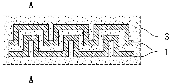
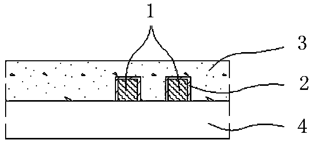
[0024] Such as figure 1 and figure 2 The circuit board manufacturing method with embedded capacitors shown is characterized in that it includes the steps of: wet film coating / dry film lamination, exposure, development, line etching, film removal, surface treatment, printing, and baking.

[0025] Specifically include the following steps:

[0026] Step A: Coating wet film / laminating dry film on the copper foil surface of the circuit board;

[0027] Step B: Exposing and developing to form the protective layer of the required ordinary circuit pattern and the parallel circuit of the capacitor plate;

[0028] Step C: removing the copper foil without protective layer by etching, leaving the required ordinary copper lines and the parallel lines 1 of the capacitor plates;

[0029] Step D: remove the film, remove the surface protection layer, and obtain the required ordinary circuit and the parallel circuit 1 of the capacitor plate;

[0030] Step E: Carrying out tinning surface tre...


PUM

PropertyMeasurementUnit
distanceaaaaaaaaaa

Abstract

The invention relates to a circuit board with an embedded capacitor and a manufacturing method thereof and belongs to the technical field of circuit board manufacturing. The method comprises steps ofwet film coating / dry film lamination, exposure, development, line etching, film stripping, surface treatment, printing and baking. The method is advantaged in that capacitor polar plates are manufactured together while a circuit is manufactured through an etching method, ink with a high dielectric constant is selected for printing in the printing process, the capacitor is directly formed in the manufacturing process of the circuit board, the capacitor does not need to be manufactured independently, the process is simple, and the cost can be greatly reduced. The capacitor is directly formed onthe circuit board, the process is simple, accurate alignment assembly is not needed, and the cost is reduced. Other material packaging is not needed, and the size is reduced. The area of the capacitorplate can be easily changed by changing the length of the parallel lines, and thereby capacitors with different capacitance values are manufactured. The method has no requirement on a material of theinsulating base material and can be suitable for all base materials.

Description

technical field [0001] The invention relates to a circuit board with a built-in capacitor and a manufacturing method thereof, belonging to the technical field of circuit board manufacturing. Background technique [0002] In recent years, with the development of miniaturization of electronic equipment, the size requirements of circuit board packaging also tend to be miniaturized. In order to meet this requirement, it is necessary to reduce not only the size of the circuit board itself, but also the size of the electronic components on the circuit board. [0003] Capacitor is one of the electronic components widely used in electronic equipment. Its basic principle is to charge and discharge, communicate with AC and block DC. According to this principle, it has many uses, such as coupling, bypass, filtering, tuning loop, energy conversion, control, etc. Capacitance is an indispensable configuration during the operation of the circuit board. From the structure of the capacitor...

Claims


Application Information

Patent Timeline
Patent Type & Authority Applications(China)
IPC IPC(8): H05K1/16H05K3/06H05K3/24H01G4/005H01G4/06
CPCH01G4/005H01G4/06H05K1/162H05K3/06H05K3/24
Inventor 方磊王健孙彬沈洪李晓华
Owner 江苏上达半导体有限公司
Learn More