Scanning interference photoetching system

A lithography system and scanning interference technology, applied in the field of optical instruments and meters, can solve the difficulties of phase solution, subdivision and direction judgment, poor anti-interference ability, difficult to achieve high-precision measurement, and difficult to realize high-precision variable-period grating manufacturing, etc. problem, to achieve the effect of high laser utilization rate and high locking precision

Active Publication Date: 2020-02-25
TSINGHUA UNIV +1
View PDF4 Cites 11 Cited by
  • Summary
  • Abstract
  • Description
  • Claims
  • Application Information

AI Technical Summary

Problems solved by technology

The measurement signal of the dual-channel homodyne heterodyne phase meter used is a DC signal, which has poor anti-interference ability and is difficult to achieve high-precision measurement. It is also difficult to solve the phase, subdivide and judge the direction, which cannot meet the needs of high-precision locking
[0007] U.S. Patent No. 6,882,477B1 discloses a scanning interference lithography system. The lithography system uses two collimated small-sized beams to interfere to form an interference pattern exposure. The exposure beam is focused by a lens to achieve a change in exposure angle, thereby To achieve variable-period interference lithography, the system adopts a pattern control system based on heterodyne measurement method, through which the phase detection of the exposure beam is fed back to the processor to control the acousto-optic modulator to achieve pattern locking. Motion errors will be generated during the process, resulting in dynamic drift of the grating pattern relative to the substrate; the patent also discloses a scanning interference lithography technology. When , the beam offset separates the measurement signals, making it impossible to achieve high-precision control of the interference pattern
[0008] From the above, it can be seen that the scanning interference lithography in the prior art has certain limitations, and it is difficult to realize high-precision variable-period grating manufacturing

Method used


Image

  • Scanning interference photoetching system
  • Scanning interference photoetching system
  • Scanning interference photoetching system

Examples


Embodiment Construction

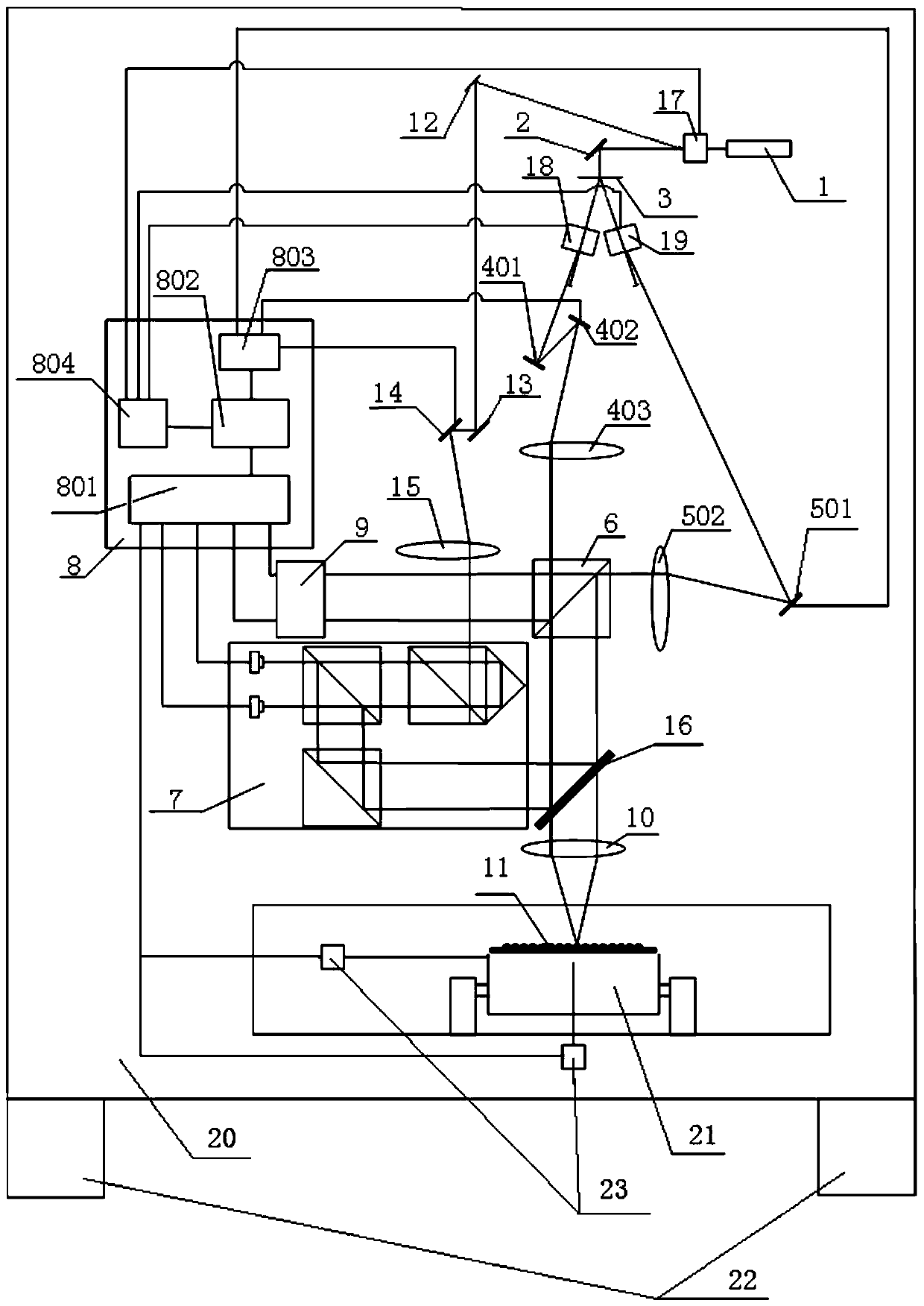
[0035] In order to further illustrate the technical means and effects of the present invention for solving technical problems, the present invention will be further described in detail below in conjunction with the accompanying drawings and specific embodiments. It should be noted that the provided accompanying drawings are schematic and mutually exclusive They are not drawn to scale or scale, and therefore the drawings and specific examples are not intended to limit the scope of protection claimed by the invention.

[0036] Such as figure 1 An optional embodiment of the scanning interference lithography system shown, the system includes:

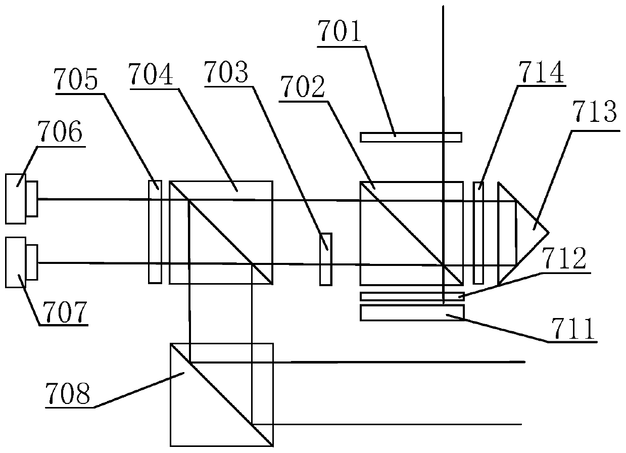
[0037] Heterodyne optical path: the laser light emitted by the laser 1 passes through the first phase modulator 17 to separate the zero-order diffracted light and the first-order diffracted light, wherein the first-order diffracted light passes through the third reflector 12, the fourth reflector 13 and the third reflector in turn. After b...


PUM


Abstract

The invention belongs to the technical field of optical instruments and meters, and provides a scanning interference photoetching system, which comprises a heterodyne light path, a first interferencelight path, a second interference light path, a motion platform and a control subsystem, wherein the motion platform is used for bearing a substrate, the displacement of the motion platform is measured by a displacement measuring interferometer, and the first beam of light and the second beam of light are focused, interfered and exposed on the substrate; the control subsystem generates an instruction according to various measurement information, adjusts the angle of a corresponding device or the phase of a light beam, and completes locking of the phase drift of the interference exposure fringes of the first light beam and the second light beam. The scanning interference photoetching system disclosed by the invention has the advantages of high fringe pattern locking precision, high laser utilization rate and the like; a heterodyne phase meter is used for measuring the phase of an exposure light beam, a displacement measuring interferometer is used for measuring the motion error of a motion platform, the control subsystem is used for compensating and controlling exposure interference fringes, and the system can be used for manufacturing large-area high-precision dense grid line gradient periodic gratings.

Description

technical field [0001] The invention belongs to the technical field of optical instruments and meters, in particular to a scanning interference photolithography system. Background technique [0002] In recent years, major engineering projects such as large-scale astronomical telescopes, inertial confinement nuclear fusion laser ignition systems, photolithography systems, etc. have continuously increased the performance requirements of grating devices, and their indicators are developing towards nanometer-level precision and sub-million-level grid line density. . At the same time, the application types are more diverse, including two-dimensional gratings, curved variable-period gratings, etc. [0003] As an important technology for manufacturing micro-nano array devices, scanning interference lithography can realize the grating manufacturing of large-scale and high-precision dense grid lines. Its core is to expose the interference pattern generated by multi-beam laser interf...

Claims


Application Information

Patent Timeline
Patent Type & Authority Applications(China)
IPC IPC(8): G03F7/20
CPCG03F7/70191G03F7/70408G03F7/70725G03F7/7085
Inventor 王磊杰朱煜张鸣徐继涛成荣郝建坤杨开明李鑫高思齐范玉娇
Owner TSINGHUA UNIV
Why Eureka
Try Eureka