Display panel and manufacturing method thereof

A display panel and film technology, which is applied in semiconductor/solid-state device manufacturing, electrical components, electric solid-state devices, etc., can solve problems such as cracks in metal wiring, achieve strong conduction direction, meet user needs, and facilitate graphics Effect

Inactive Publication Date: 2020-02-28
WUHAN CHINA STAR OPTOELECTRONICS SEMICON DISPLAY TECH CO LTD
View PDF6 Cites 0 Cited by
  • Summary
  • Abstract
  • Description
  • Claims
  • Application Information

AI Technical Summary

Problems solved by technology

However, the metal traces currently used in OLEDs mainly include molybdenum (Mo), titanium (Ti), and aluminum (Al) with high elastic modulus. Although metals are more resistant to bending than inorganic films, but with With the continuous reduction of bending radius and the continuous increase of product bending times, it is difficult for the currently used metal materials to meet more and more stringent requirements. Under the current technical conditions, metal traces are prone to cracks after bending

Method used


Image

  • Display panel and manufacturing method thereof
  • Display panel and manufacturing method thereof

Examples


Embodiment 1

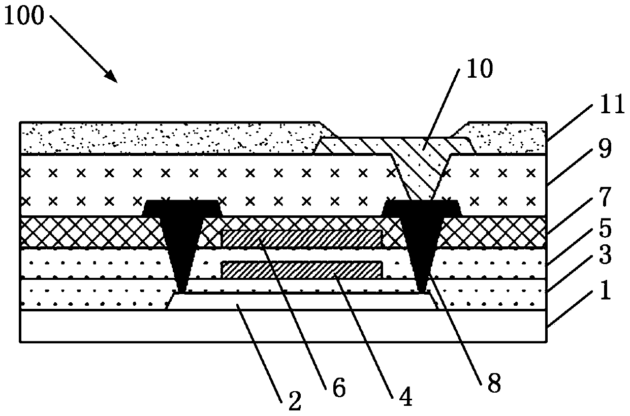
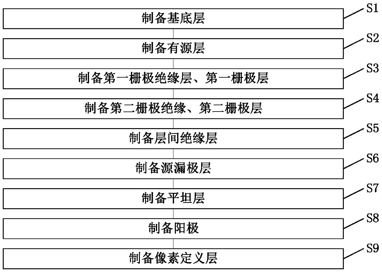
[0033] like figure 1 As shown, a display panel 100, which includes: a base layer 1 and a conductive layer, wherein the conductive layer is a conductive polymer film; the conductive layer can be the first gate layer 4, the second gate layer 6 or One or more of the source and drain layers 8 .

[0034] The display panel 100 further includes: an active layer 2 , a first gate insulating layer 3 , a second gate insulating layer 5 , an interlayer insulating layer 7 , a flat layer 9 , an anode 10 and a pixel definition layer 11 . Wherein the active layer 2 is disposed on the base layer 1; the first gate insulating layer 3 is disposed on the active layer 2; the first gate layer 4 is disposed on the first gate on the pole insulating layer 3; the second gate insulating layer 5 is disposed on the first gate layer 4; the second gate layer 6 is disposed on the second gate insulating layer 5; the The interlayer insulating layer 7 is disposed on the second gate layer 6; the source and drain...


PUM


Abstract

The present invention relates to a display panel and a manufacturing method thereof. The display panel utilizes the advantage that a conductive polymer can form a film over a large area, facilitates patterning, and has an electrical conductivity that is comparable to that of metal and not decreasing with an increase in temperature, excellent bending resistance, good conductance direction and the like. A conductive polymer material replaces the metal material of wires in the display panel to satisfiy the requirements for both conductivity and bending resistance.

Description

technical field [0001] The invention relates to the field of display technology, in particular to a display panel and a preparation method thereof. Background technique [0002] OLED (full name in English: Organic Light-Emitting Diode, referred to as OLED) devices are also called organic electro-laser display devices and organic light-emitting semiconductors. The basic structure of an OLED is a thin, transparent indium tin oxide (ITO) with semiconducting properties connected to the positive electrode of electricity, plus another metal surface cathode, wrapped into a sandwich structure. The whole structural layer includes: hole transport layer (HTL), light emitting layer (EL) and electron transport layer (ETL). When the power is supplied to an appropriate voltage, positive holes and surface cathode charges will combine in the light-emitting layer, and under the action of Coulomb force, they will recombine with a certain probability to form excitons (electron-hole pairs) in a...

Claims


Application Information

Patent Timeline
Patent Type & Authority Applications(China)
IPC IPC(8): H01L27/32H01L27/12H01L21/77
CPCH01L27/1244H10K59/179H10K59/1201H01L27/1218H01L21/288H01L27/1259H01L29/45H01L29/4908
Inventor 周志伟
Owner WUHAN CHINA STAR OPTOELECTRONICS SEMICON DISPLAY TECH CO LTD
Why Eureka
Try Eureka