Ultraviolet light source packaging element
A technology for packaging components and ultraviolet light sources, which is applied in the direction of electrical components, semiconductor devices, circuits, etc., can solve problems such as air bubbles that cannot be eliminated, affect light extraction efficiency, and deformation of optical components, so as to achieve no air residue, improve fixation, and reduce total reflection. Effect
- Summary
- Abstract
- Description
- Claims
- Application Information
AI Technical Summary
Problems solved by technology
Method used
Image
Examples
Embodiment 1
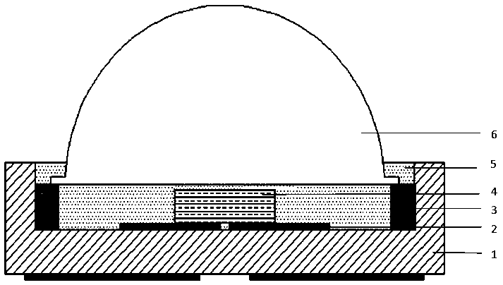
[0042] Please refer to the attached figure 2 , the present embodiment provides an ultraviolet LED packaging structure, which includes: a base frame 1, an optical element 6, and an LED chip 4; the base frame 1 has a groove in the center, and the bottom of the groove fixes the LED chip 4 ; Wherein the pedestal groove is filled with fluorine-containing resin 5, the optical element 6 falls into the groove and is located above the LED chip 4, there is a gap between the edge of the optical element 6 and the inner sidewall of the groove The gap, the gap is filled with fluorine-containing resin 5, the gap between the edge of the optical element 6 and the inner side wall of the groove realizes the elimination of air bubbles, and the fluorine-containing resin 5 covers part of the upper surface of the optical element through the gap to form a buckle effect.
[0043]Specifically, the base frame 1 is preferably an integrally formed ceramic material or a combined structure in which the bo...
Embodiment 2
[0065]As a modification of Example 1, as Figure 7 The bottom of the groove shown is provided with a continuous annular step 3 against the side wall, the height of the annular step 3 is the same, and part of the edge of the optical element 6 is placed on the step 3, and the height of the step 3 is It is greater than the height of the chip and lower than the height of the sidewall of the groove. Through the setting of the step height, the distance between the chip and the optical element can be effectively controlled, so that the light emitting angle can be effectively controlled to radiate at an angle close to the vertical as far as possible. An adhesive layer is formed between the optical element and the step, and the material of the adhesive layer is the same as or different from that of the fluororesin, or the adhesiveness of the adhesive layer is higher than that of the fluororesin. The adhesive layer here can be made of one or more layers of materials. The edge of the op...
Embodiment 3
[0067] This embodiment provides an ultraviolet light source package element different from the previous embodiment, such as Figure 8 As shown, it includes: a base frame 1, an optical element 6 and an LED chip 4; the base frame 1 has a groove in the center, and the bottom of the groove fixes the LED chip 4; the edge of the optical element 6 is placed on the On the step in the groove of the base frame, the optical element preferably has a platform on the edge, the platform is placed on the step, an adhesive layer is arranged between the platform and the step, and the adhesive force of the adhesive layer is preferably higher than that of the fluorine-containing resin, The fluorine-containing resin 5 fills the groove of the base frame, the optical element has a hole 8, and the fluorine-containing resin fills the hole and covers the outer surface around the hole. Through the fluorine-containing resin overflow hole, the snap action between the optical element and the fluorine-conta...
PUM
| Property | Measurement | Unit |
|---|---|---|
| surface roughness | aaaaa | aaaaa |
| refractive index | aaaaa | aaaaa |
| wavelength | aaaaa | aaaaa |
Abstract
Description
Claims
Application Information


