Adjustable perfect wave absorber based on graphene photonic crystal structure
A photonic crystal and wave absorber technology, applied in the field of wave absorber materials, can solve the problems of adding a sandwich photonic crystal structure, etc., and achieve the effect of saving manufacturing costs
- Summary
- Abstract
- Description
- Claims
- Application Information
AI Technical Summary
Problems solved by technology
Method used
Image
Examples
Embodiment Construction
[0016] The technical solutions of the present invention will be clearly and completely described below in conjunction with the accompanying drawings in the embodiments. Apparently, the described embodiments are only some of the embodiments of the present invention, not all of them. Based on the embodiments of the present invention, all other embodiments obtained by persons of ordinary skill in the art without making creative efforts belong to the protection scope of the present invention.
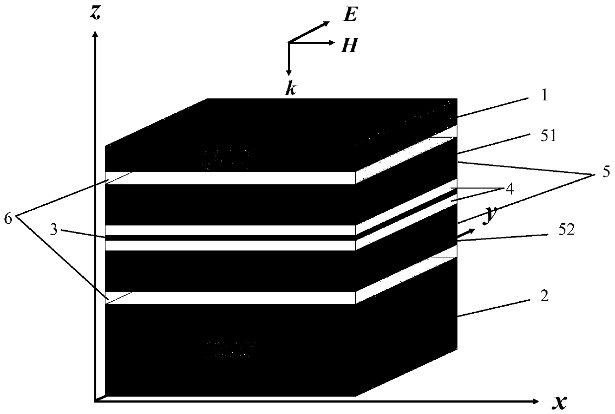
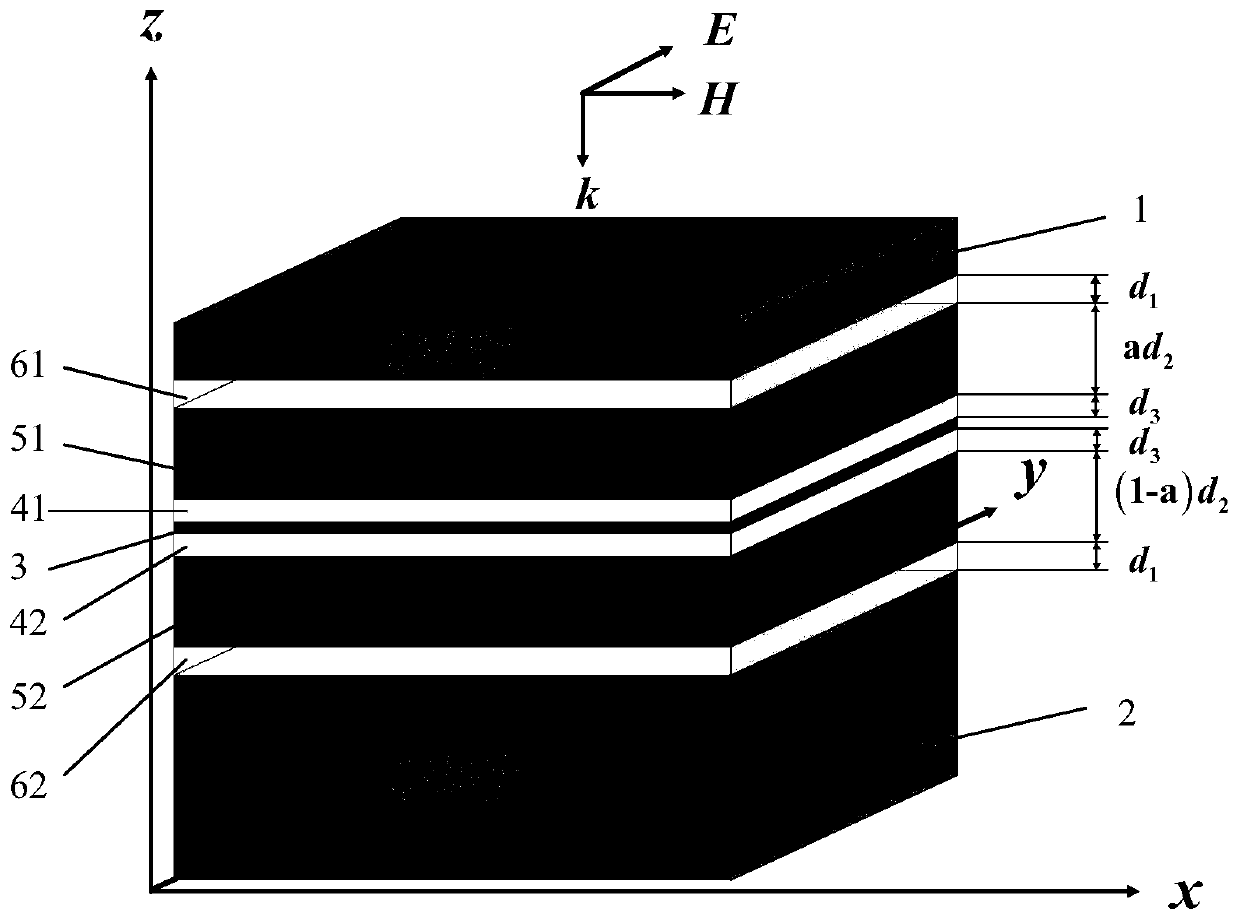
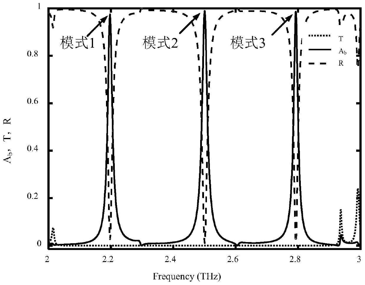
[0017] The invention is an adjustable perfect absorber based on graphene photonic crystal structure, including triple nested FP resonant cavity, top mirror (A / B) n , bottom mirror (B / A) m Three parts, in which the triple nested FP resonator is composed of three layers of photonic crystal defect cavities sandwiched, and the first layer of cavity is located around the graphene monolayer, and the material of the first layer of cavity is silicon dioxide; it is attached to The defect cavity aro...
PUM
 Abstract
Description
Claims
Application Information


