Method for high-effectively regulating the dislocation density of local area of CVD monocrystal diamond

A single crystal diamond, local area technology, applied in the direction of single crystal growth, single crystal growth, chemical instruments and methods, etc., can solve the problem of inability to locally control the inhomogeneity of the diamond substrate, and achieve the improvement of crystal quality and uniformity, Efficient processing effect

Active Publication Date: 2020-03-31
WUHAN UNIV
View PDF3 Cites 9 Cited by
  • Summary
  • Abstract
  • Description
  • Claims
  • Application Information

AI Technical Summary

Problems solved by technology

[0003] The purpose of the present invention is to provide a method for efficiently controlling the dislocation density of CVD single crystal diamond in local areas, so as to solve the problem that the existing methods can only be processed as a whole, and cannot be locally adjusted for the inhomogeneity of the diamond substrate.

Method used


Image

  • Method for high-effectively regulating the dislocation density of local area of CVD monocrystal diamond
  • Method for high-effectively regulating the dislocation density of local area of CVD monocrystal diamond
  • Method for high-effectively regulating the dislocation density of local area of CVD monocrystal diamond

Examples


Embodiment 1

[0039] The method for efficiently controlling the dislocation density in the local area of ​​CVD single crystal diamond has the following steps:

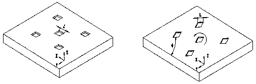
[0040] (1) Detection of dislocation density and distribution in diamond substrates

[0041] a. Domestically produced type Ib HPHT diamond is used as the substrate material, and its size is 3mm×3mm×0.5mm. Use H 2 SO 4 / KNO 3 Mixed solution heat treatment, acetone ultrasonic cleaning, ethanol ultrasonic cleaning, deionized water ultrasonic cleaning and other steps to clean the diamond substrate, the purpose is to remove the residual metal, graphite, organic matter and other pollutants on the surface of the diamond sample;

[0042] b. H for about 1h on the diamond substrate 2 / O 2 (O 2 / H 2 2%) plasma etching treatment;

[0043] c. Use 3D optical profiler, atomic force microscope or differential interference microscope to characterize the etched morphology of the diamond substrate surface, and use an orthogonal polarizing micro...

Embodiment 2

[0058] The method for efficiently controlling the dislocation density in the local area of ​​CVD single crystal diamond has the following steps:

[0059] (1) Detection of dislocation density and distribution in diamond substrates

[0060] a. Domestically produced type Ib HPHT diamond is used as the substrate material, and its size is 3mm×3mm×0.5mm. The diamond substrate is cleaned by aqua regia heat treatment, acetone ultrasonic cleaning, ethanol ultrasonic cleaning, deionized water ultrasonic cleaning and other steps to remove metal, graphite, organic matter and other pollutants remaining on the surface of the diamond sample;

[0061] b. H for about 1h on the diamond substrate 2 / O 2 (O 2 / H 2 2%) plasma etching treatment;

[0062] c. Use 3D optical profiler, atomic force microscope or differential interference microscope to characterize the etched morphology of the diamond substrate surface, and use an orthogonal polarizing microscope system to detect abnormal birefring...


PUM

PropertyMeasurementUnit
thicknessaaaaaaaaaa
thicknessaaaaaaaaaa
lengthaaaaaaaaaa

Abstract

The invention discloses a method for high-effectively regulating the dislocation density of local area of CVD monocrystal diamond. In the method, composite technologies such as plasma etching, surfaceappearance detection and orthogonal polarization imaging, etc., a high-dislocation density area in a diamond substrate can be rapidly and destructively determined; by using high-energy particle beamssuch as femtosecond laser, the high-dislocation density area in the diamond substrate is patterned flexibly and high-effectively. With combination of selection and arrangement of a mask material in agraphical area, the method can block the extension of the dislocation of bottom area of the processed pattern to the CVD diamond growing layer, regulate the extension direction of the dislocation line on the side area of the pattern, and release the stress during the process of growing the graphical area, thus reducing the dislocation density and residual stress of the local area in the CVD diamond growing layer effectively, achieving pertinent regulation of defects and crystallization quality of the growing layer, and improving the growing uniformity and crystal quality of the CVD diamond.

Description

technical field [0001] The invention belongs to the field of single-crystal diamond growth, and in particular relates to a method for efficiently regulating the dislocation density of local regions in CVD diamond based on rapid detection of defects in diamond and micro-nano processing of high-energy particle beams such as femtosecond lasers. Background technique [0002] Diamond has excellent physical and chemical properties, its band gap is about 5.5 eV, and its thermal conductivity is as high as 22 W cm -1 ·K -1 , and has the characteristics of high breakdown voltage, small dielectric constant and high radiation hardness, which is obviously superior to the third-generation semiconductor materials such as GaN and SiC (Fu Fangbin, Jin Peng, Liu Yali, Gong Meng, Wu Ju, Wang Zhanguo. MPCVD growth semiconductor Research status of diamond materials [J]. Micro-Nano Electronics Technology, 2016, 53(09): 571-581+587.), is the key material for future chip manufacturing. Based on...

Claims


Application Information

Patent Timeline
Patent Type & Authority Applications(China)
IPC IPC(8): C30B25/00C30B29/04C23C16/02C23C16/04C23C16/27
CPCC23C16/02C23C16/0245C23C16/042C23C16/27C23C16/279C30B25/00C30B29/04
Inventor 刘胜吴改汪启军东芳曹强甘志银
Owner WUHAN UNIV
Why Eureka
Try Eureka