Processing equipment for semiconductor or photovoltaic materials

A photovoltaic material and processing device technology, which is applied in semiconductor devices, semiconductor/solid-state device manufacturing, photovoltaic power generation, etc., can solve the problems of large graphite ark, high defective rate, and black edges on silicon wafers, etc., to improve the resistance Compressive properties and service life, improved compression resistance, reasonable design effects

Active Publication Date: 2022-04-22
LAPLACE RENEWABLE ENERGY TECH CO LTD
View PDF9 Cites 0 Cited by
  • Summary
  • Abstract
  • Description
  • Claims
  • Application Information

AI Technical Summary

Problems solved by technology

[0003] The following problems exist in the current equipment: the graphite ark is usually large in size, generally reaching about 2 meters, and the electric field will have a large difference from the tail to the front of the entire graphite ark, and it is difficult to obtain a uniform electric field
Since the silicon wafer needs to be placed vertically, the surface of the silicon wafer will not be tightly bonded to the surface of the boat board, which will lead to poor electrical conductivity of the silicon wafer. The risk of rewinding, resulting in an increase in the rate of defective products
The overall production capacity of the equipment is still low
[0004] Moreover, the furnace door of the corresponding existing equipment is sealed by the way that the sealing plate is in contact with the furnace frame, and the sealing plate is a buckle type, that is, the sealing plate passes through The buckle is fixed on the furnace door. When the furnace door is not tightly sealed, the operator pushes the sealing plate forward to seal by tapping the buckle. However, after a long period of use, the position where the sealing plate contacts the furnace frame is severely worn. When the furnace door and the furnace frame are sealed by the sealing plate, the seal will not be tight, which will cause smoke from the furnace door, affect the environmental sanitation, and also have a serious impact on the economic and social benefits of the enterprise

Method used


Image

  • Processing equipment for semiconductor or photovoltaic materials
  • Processing equipment for semiconductor or photovoltaic materials
  • Processing equipment for semiconductor or photovoltaic materials

Examples


Embodiment

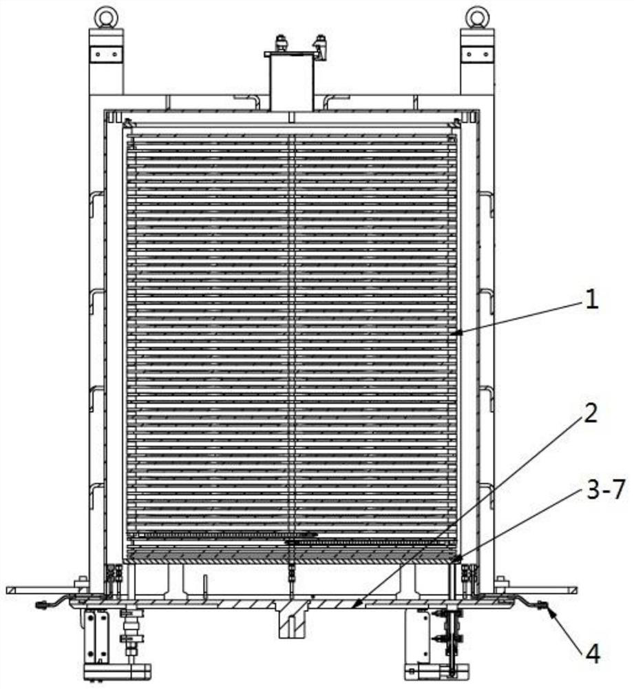
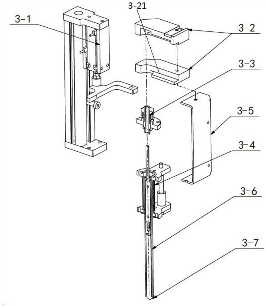
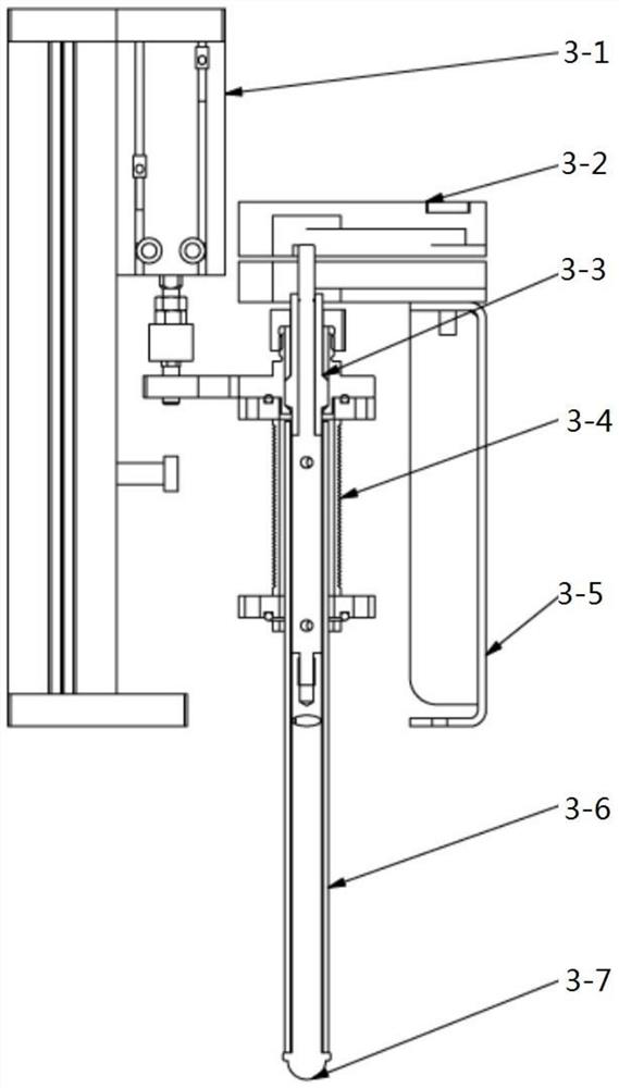
[0035] Such as Figure 1 to Figure 6 As shown, the semiconductor or photovoltaic material processing device includes an ark structure, a semiconductor or photovoltaic material processing structure; the ark structure is placed on the semiconductor or photovoltaic material processing structure, the electrode structure of the semiconductor or photovoltaic material processing structure and the first The two electrode columns 10 are connected; the processing equipment of semiconductor or photovoltaic materials includes a furnace body 1, a furnace door 2, and an electrode structure is arranged on the furnace door 2, and the electrode structure includes a first electrode column 3-7, an electrode body 3-5 and Insulation Materials. The first electrode column 3-7 is connected to the electrode body 3-5, and the insulating material covers the side of the first electrode column 3-7. By insulating and covering the electrode columns, only the two ends of the first electrode columns 3-7 are ...


PUM


Abstract

Semiconductor or photovoltaic material processing device, including ark structure, semiconductor or photovoltaic material processing structure; the ark structure is placed on the semiconductor or photovoltaic material processing structure, and the electrode structure of the semiconductor or photovoltaic material processing structure is connected to the electrode column of the ark structure The processing structure of semiconductor or photovoltaic materials includes a furnace body, a furnace door, a furnace door, an electrode structure is arranged on the furnace door, and an adjustment device is arranged on the furnace door. The adjustment device includes an arc-shaped contact surface and a support block, and the arc-shaped contact surface is arranged on Between the supporting block and the furnace door, a structure matching the arc-shaped contact surface is provided at the corresponding position of the supporting block or the furnace door; It is placed vertically and can quickly adjust the furnace door to achieve semiconductor or photovoltaic material processing equipment with good sealing effect.

Description

technical field [0001] The invention relates to the field of semiconductor or photovoltaic material processing, more specifically, it relates to a semiconductor or photovoltaic material processing device. Background technique [0002] Semiconductor or photovoltaic materials are widely used in electronics, new energy and other industries. Semiconductor and photovoltaic materials usually require chemical treatment before they can be applied to products. CVD technology is one of the processing methods. CVD is chemical vapor deposition. CVD technology is currently It has been widely used in the processing of semiconductor or photovoltaic materials. Common processing equipment includes PECVD, LPCVD, APCVD, etc. In addition to CVD, there are also diffusion processes, such as phosphorus diffusion, boron diffusion, etc., which can use gas diffusion to treat raw materials. Processing. At present, there are many related equipment in the industry. The corresponding equipment can be sel...

Claims


Application Information

Patent Timeline
Patent Type & Authority Patents(China)
IPC IPC(8): H01J37/32H01L21/673H01L31/18
CPCH01J37/32513H01J37/32568H01L21/6732H01L31/186Y02P70/50Y02E10/50
Inventor 刘群徐栋林佳继朱太荣林依婷
Owner LAPLACE RENEWABLE ENERGY TECH CO LTD
Why Eureka
Try Eureka