Multichannel parallel photoelectric detection circuit structure
A technology of photoelectric detection and circuit structure, applied in the field of optical communication, can solve the problems of low detection efficiency, reduced signal-to-noise ratio, signal submergence, etc., and achieve the effects of improving detection efficiency, improving dynamic range, and reducing circuit noise floor
- Summary
- Abstract
- Description
- Claims
- Application Information
AI Technical Summary
Problems solved by technology
Method used
Image

Examples
Embodiment Construction
[0035] In order to make the object, technical solution and advantages of the present invention clearer, the present invention will be further described in detail below in conjunction with the accompanying drawings and embodiments. It should be understood that the specific embodiments described here are only used to explain the present invention, not to limit the present invention.
[0036] In the description of the present invention, the terms "inner", "outer", "longitudinal", "transverse", "upper", "lower", "top", "bottom", "left", "right", "front" ", "rear" and other indicated orientations or positional relationships are based on the orientations or positional relationships shown in the drawings, and are only for the convenience of describing the present invention and do not require that the present invention must be constructed and operated in a specific orientation, so it should not be understood as Limitations on the Invention.
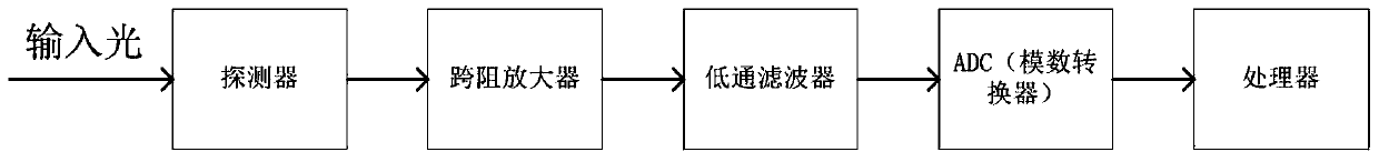
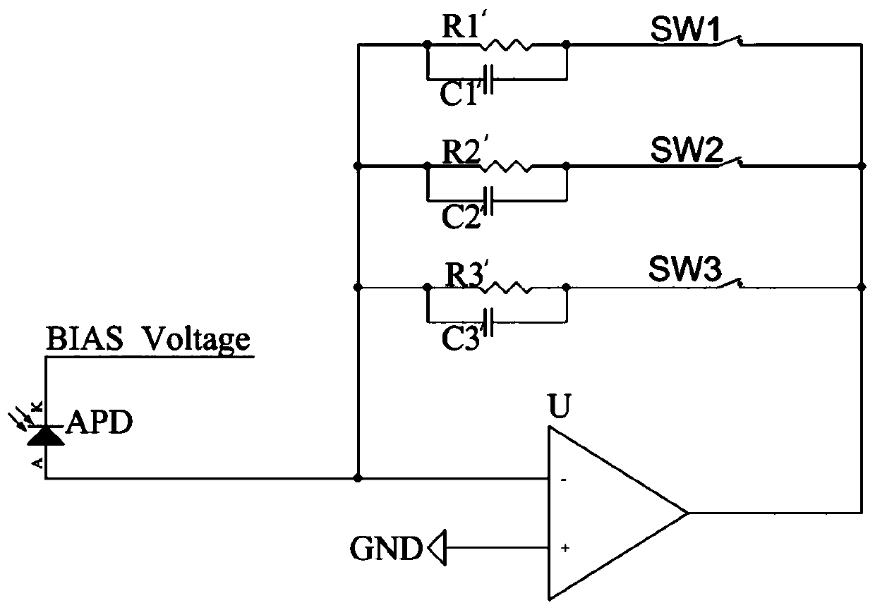
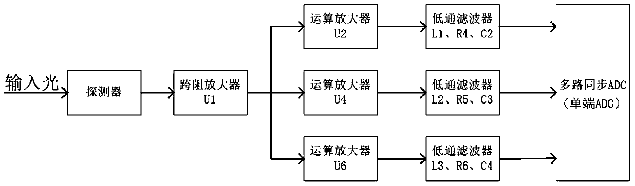
[0037] In each embodiment of the present ...
PUM
 Abstract
Description
Claims
Application Information