

Circuit and electronic device
A technology of electronic devices and circuits, applied in the direction of electric solid devices, circuits, electronic switches, etc., can solve problems such as increasing the normal operating voltage of circuits
- Summary
- Abstract
- Description
- Claims
- Application Information
AI Technical Summary
Problems solved by technology
Method used
Image

Examples
Embodiment approach 1
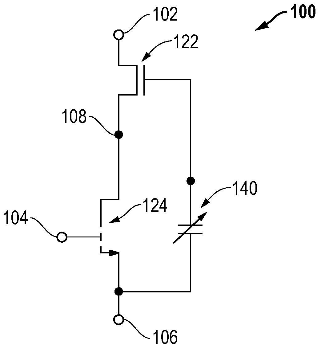
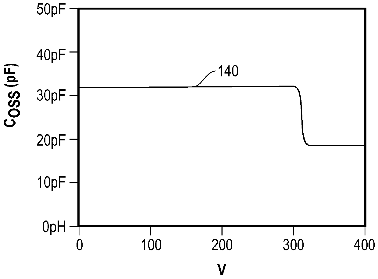
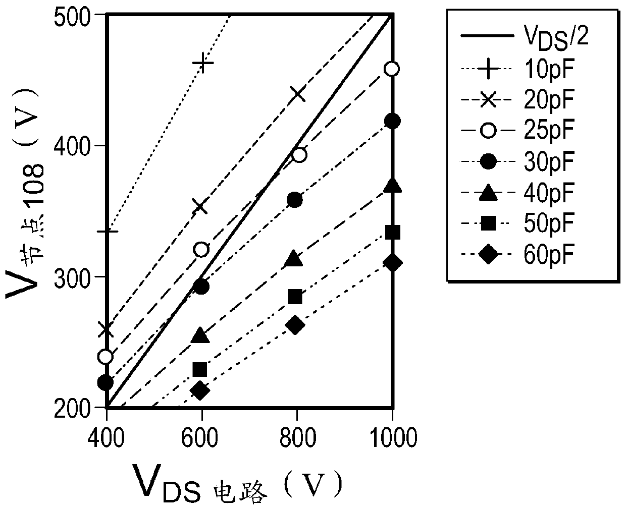
[0082] Embodiment 1. A circuit may include: a first high electron mobility transistor; a second high electron mobility transistor, wherein the drain of the first high electron mobility transistor is coupled to the source of the second high electron mobility transistor and a first variable capacitor, wherein the first electrode of the first variable capacitor is coupled to the source of the first high electron mobility transistor, and the second electrode of the first variable capacitor is coupled to the second high electron mobility rate transistor gate.
Embodiment approach 2
[0083] Embodiment 2. The circuit of embodiment 1, wherein the first high electron mobility transistor is an enhancement transistor and the second high electron mobility transistor is a depletion transistor.
Embodiment approach 3
[0084] Embodiment 3. The circuit of embodiment 1, further comprising a first diode and a second diode, wherein the cathode of the first diode is coupled to the second electrode of the first variable capacitor, the first The anode of the diode is coupled to the anode of the second diode and the cathode of the second diode is coupled to the drain of the first high electron mobility transistor and the source of the second high electron mobility transistor.
PUM
| Property | Measurement | Unit |
|---|---|---|
| capacitance | aaaaa | aaaaa |
| capacitance | aaaaa | aaaaa |
| breakdown voltage | aaaaa | aaaaa |
Abstract
Description
Claims
Application Information