

Novel ark structure
An ark and a new type of technology, applied in the field of new ark structures, can solve the problems of the surface of the silicon wafer and the surface of the ark board being not tightly attached, it is difficult to obtain a uniform electric field, and the production capacity is low.
- Summary
- Abstract
- Description
- Claims
- Application Information
AI Technical Summary
Problems solved by technology
Method used
Image

Examples
Embodiment
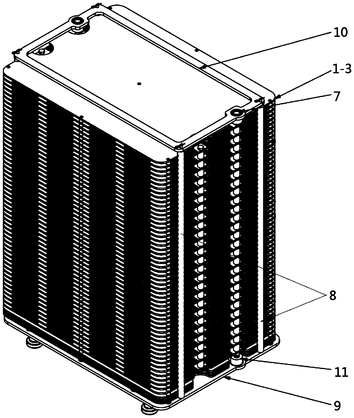
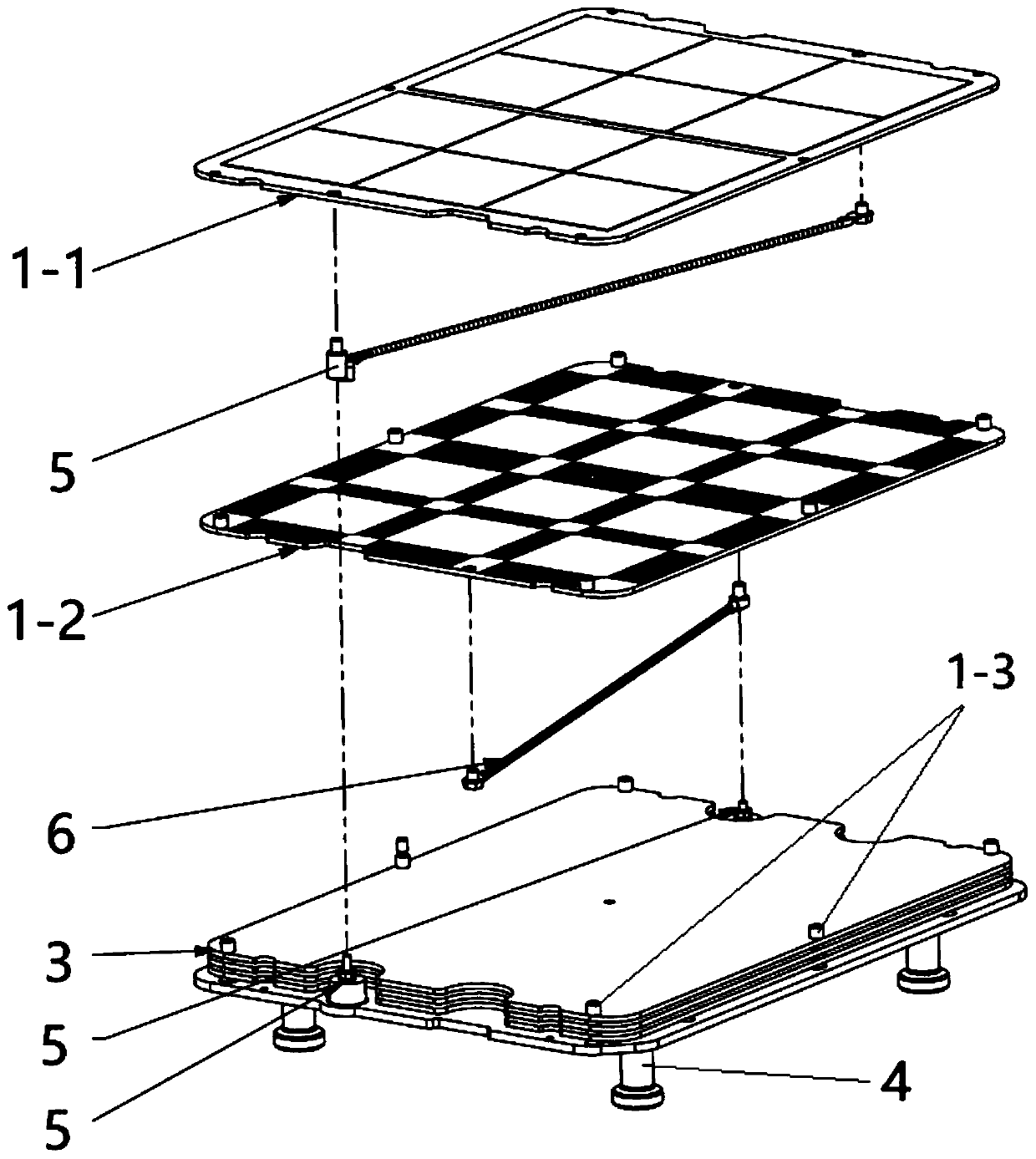
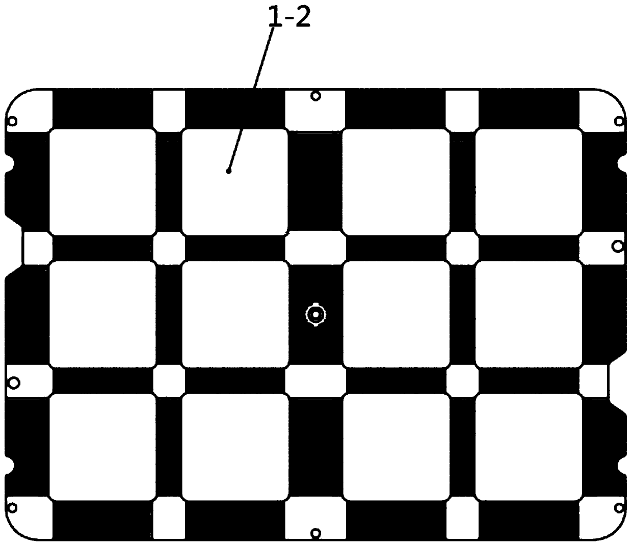
[0027] Such as figure 1 As shown, the novel ark structure includes an ark frame 7, a first boat plate 1-1, a second boat plate 1-2, and a smoothing plate 3; the top and bottom of the ark support are provided with a smoothing plate 3; multiple first boats The plate 1-1 and the second boat plate 1-2 are arranged at intervals between the top even flow plate 3 and the bottom even flow plate 3 . The space for placing alternately arranged first boat boards 1-1 and second boat boards 1-2 is provided by the ark frame 7 as a whole. Among them, the arrangement of the flow uniform plate 3 eliminates the situation that the top and bottom processing effects are not good.
[0028] The ark frame 7 includes a fixing column 8 , a bottom plate 9 and a top fixing frame 10 . The fixing column 8 connects the bottom plate 9 and the top fixing frame 10; both ends of the fixing column 8 are fixed on the bottom plate 9 and the top fixing frame 10 by welding. Electrode column fixing holes 11 are pro...
PUM
 Abstract
Description
Claims
Application Information