

Method and system for transferring large number of MicroLED chips
A chip and a huge amount of technology, which is applied in the field of mass transfer of MicroLED chips, can solve the problems of MicroLED chips that cannot guarantee accurate positioning and are difficult to control, and achieve the effects of batch processing, easy control, and strong feasibility
- Summary
- Abstract
- Description
- Claims
- Application Information
AI Technical Summary
Problems solved by technology
Method used
Image

Examples
Embodiment Construction
[0055] In order to make the object, technical solution and advantages of the present invention clearer, the present invention will be further described in detail below in conjunction with the accompanying drawings.
[0056] Such as figure 1 As shown, the present invention provides a method for mass transfer of MicroLED chips, including:
[0057] S101. Provide a substrate, the surface of the substrate is provided with a first metal layer;
[0058] The substrate may be made of glass, metal or plastic, but is not limited thereto. The surface of the substrate is provided with a first metal layer. Since the MicroLED chip needs to be transferred to the PCB board eventually, the position of the first metal layer on the substrate needs to correspond to the chip soldering point on the PCB board.
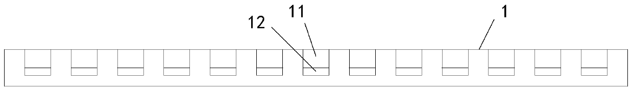
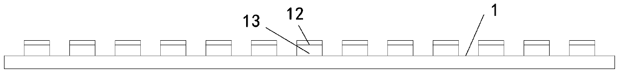
[0059] preferred, such as figure 2 As shown, the substrate 1 is a concave substrate, the concave substrate is provided with a plurality of grooves 11 , and the first metal layer 12 is dis...
PUM
| Property | Measurement | Unit |
|---|---|---|
| Thickness | aaaaa | aaaaa |
Abstract
Description
Claims
Application Information