Optical frequency response electron tunneling structure, preparation method and use thereof

A technology of electron tunneling and optical frequency, which is applied in the field of optical frequency response, can solve the problems of low optical frequency response efficiency and achieve the effects of reducing tunneling junction capacitance, enhancing absorption, and enhancing optical frequency response efficiency

Active Publication Date: 2021-11-02
THE NAT CENT FOR NANOSCI & TECH NCNST OF CHINA
View PDF7 Cites 0 Cited by
  • Summary
  • Abstract
  • Description
  • Claims
  • Application Information

AI Technical Summary

Problems solved by technology

[0006] Aiming at the problem of extremely low overall optical frequency response efficiency in the prior art, the object of the present invention is to provide an optical frequency responsive electron tunneling structure, its preparation method and application

Method used


Image

  • Optical frequency response electron tunneling structure, preparation method and use thereof
  • Optical frequency response electron tunneling structure, preparation method and use thereof
  • Optical frequency response electron tunneling structure, preparation method and use thereof

Examples


Embodiment 1

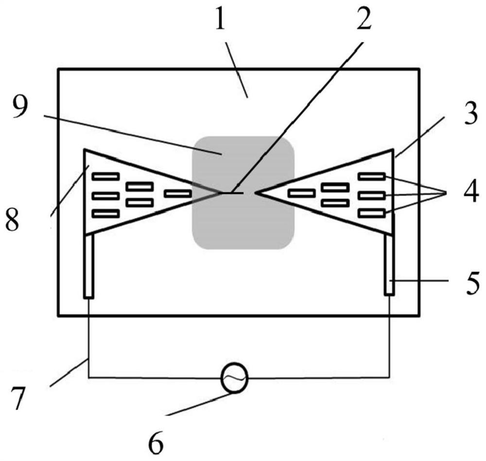
[0092] An optical frequency-responsive electron tunneling device using gold nanoribbons to enhance the electron tunneling process (for a schematic diagram of its structure, see figure 1 ):

[0093] In the structure of the optical frequency response electron tunneling device in this embodiment: the substrate 1 is SiO 2 The substrate, the electron tunneling tip 2 is a carbon nanotube with a diameter of 5 nm, the first substrate in the upper electrode 3 is an Au electrode, the nano-enhanced structure 4 is an Au nano-strip, and the in-plane lead 5 is an Al in-plane electrode. The collector 6 is a Keithley Naan ammeter, the external lead 7 is a Cu wire, the second substrate in the lower electrode 8 is the lower Au electrode, and the nano-tunneling layer 9 is Al 2 o 3 Nano tunneling layer;

[0094] Among them, Al 2 o 3 The thickness of the tunneling layer is 1 nanometer, the bow-tie optical antenna, the side length of a single regular triangle is 300nm, the diameter of the elec...

Embodiment 2

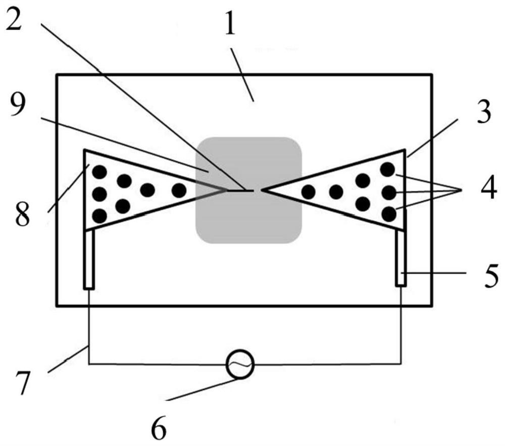
[0104] An optical frequency-responsive electron tunneling device using carbon nanotips to enhance the electron tunneling process:

[0105] The structure of the optical frequency response electron tunneling device in this embodiment is as follows image 3 As shown in the figure: substrate 1 is Al 2 o 3 The substrate, the electron tunneling tip 2 is a carbon nano tip, the first substrate in the upper electrode 3 is an upper Ag electrode, the nano-enhanced structure 4 is an Al nanoparticle, the in-plane lead 5 is an Au in-plane electrode, and the current detection and collector 6 It is a Keithley Naan ammeter, the external lead 7 is a Cu wire, the second substrate in the lower electrode 8 is a lower Ag electrode, and the nano-tunneling layer 9 is Al 2 o 3 Nanotunneling layer.

[0106] Among them, Al 2 o 3 The thickness of the tunneling layer is 5 nanometers, the diameter and length of the carbon nanometer tip are 1nm and 5 μm respectively, the characteristic size of the upp...


PUM


Abstract

The invention relates to an optical frequency response electron tunneling structure, its preparation method and application. The invention utilizes the characteristic that the time required for electron tunneling through the nano-insulation layer is on the femtosecond level, and uses a nano-enhanced structure to enhance the energy absorption of the optical frequency electromagnetic wave radiation by the antenna, thereby realizing the detection and energy collection of the optical frequency signal and enhancing the optical frequency. Response efficiency, at the same time, can realize the optical frequency response of infrared, visible or ultraviolet bands, and the response speed can exceed the existing commercial optoelectronic devices. The optical frequency responsive electronic tunneling structure of the present invention has the advantages of fast response time and a pixel area in the order of nanometer size, and can be widely used in fields such as optical frequency detection, radiation energy collection, and high-resolution imaging.

Description

technical field [0001] The invention belongs to the technical field of optical frequency response, and in particular relates to an optical frequency response electron tunneling structure, its preparation method and application. Background technique [0002] Optical frequency response refers to the physical process of transmitting infrared-visible light through a photoelectric functional structure that matches its wavelength to achieve optical frequency signal transmission and energy conversion. Its notable feature is that the rectification frequency is up to 10 13 -10 15 Hz range, exceeding the operating frequency limit of existing semiconductor materials. Since infrared-visible light is closely related to human life and production, the research on optical frequency rectification process will play a huge role in photoelectric detection, solar cells, wireless energy transmission, nanophotonics, infrared sensing imaging and other fields. For example, an optical calculator th...

Claims


Application Information

Patent Timeline
Patent Type & Authority Patents(China)
IPC IPC(8): H01L31/108H01L31/0352H01L31/0224H01L31/0216H01L31/02H01L31/18H01L27/144
CPCH01L27/1443H01L31/02005H01L31/02161H01L31/022408H01L31/03529H01L31/1085H01L31/1804Y02P70/50
Inventor 戴庆李振军李驰白冰陈科周圣涵
Owner THE NAT CENT FOR NANOSCI & TECH NCNST OF CHINA
Why Eureka
Try Eureka