

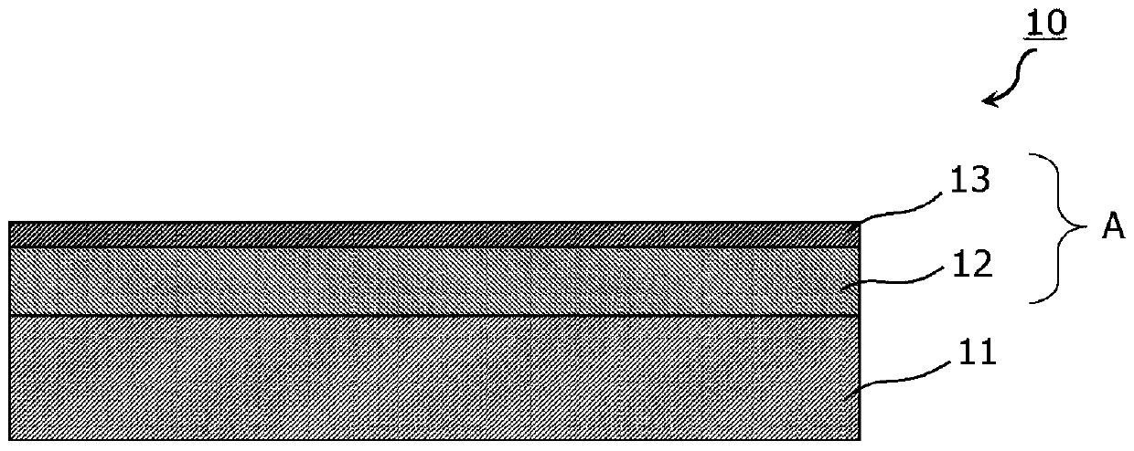
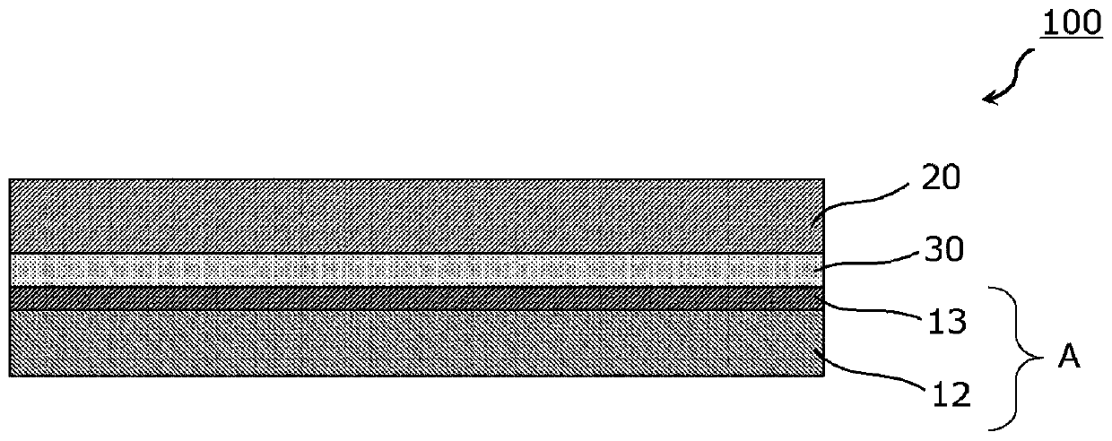
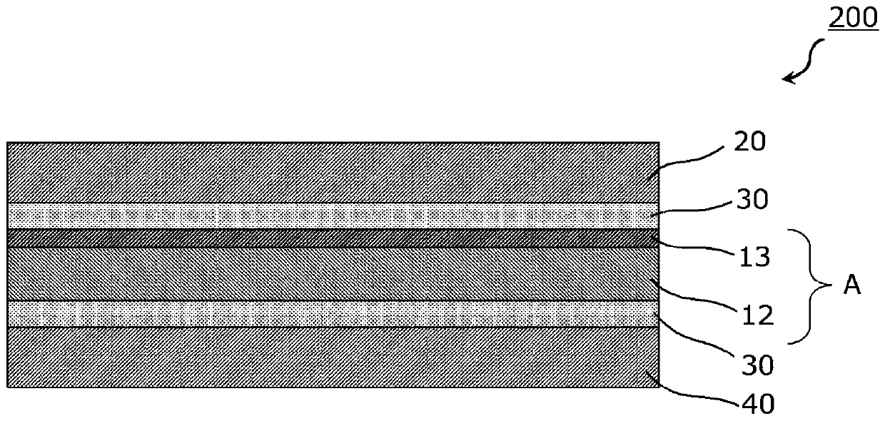
Conductive transfer film
A technology of conductive film and conductive layer, which is applied in the direction of equipment for manufacturing conductive/semiconductive layers, conductive layers on insulating carriers, circuits, etc., which can solve the problems of conductivity and transparency, which cannot be introduced, and transparent resin Problems such as barriers to bending resistance of films
- Summary
- Abstract
- Description
- Claims
- Application Information
AI Technical Summary
Problems solved by technology
Method used
Image

Examples
Embodiment 1
[0142] A polyethylene terephthalate substrate (manufactured by PANAC CO., LTD., trade name "PANA-PEEL") subjected to mold release treatment was used as a temporary support, and the following method was applied to the temporary support. A resin layer is formed.
[0143] As a binder resin, urethane-based polyfunctional acrylate A (manufactured by DIC Corporation, trade name "UNIDICELS888") and urethane-based polyfunctional acrylate B (manufactured by DIC Corporation, trade name "UNIDICELS888") were prepared. UNIDICRS28-605" is a coating composition mixed with urethane-based multifunctional acrylate A: urethane-based multifunctional acrylate B = 8:2 by weight and diluted with ethyl acetate. Use gravure The coater applied the coating composition to the release-treated surface of the above-mentioned temporary support so that the thickness after drying became 5 μm, and thereafter, the coated layer was heated at 80° C. Next, the accumulation was irradiated with a high-pressure mercur...
Embodiment 2
[0146]Let the weight ratio of urethane-based polyfunctional acrylate A and urethane-based polyfunctional acrylate B be urethane-based polyfunctional acrylate A: urethane-based polyfunctional acrylate B=2 : 8, except that, it carried out similarly to Example 1, and obtained the electroconductive film for transfer.
Embodiment 3
[0148] A polyethylene terephthalate substrate (manufactured by PANAC CO., LTD., trade name "PANA-PEEL") subjected to mold release treatment was used as a temporary support, and the following method was passed on the temporary support. method to form a liquid crystal layer.
[0149] With the following chemical formula (I) (numbers 65 and 35 in the formula represent the mol% of the monomer unit, for the sake of convenience, it is represented by a block polymer body: 20 parts by weight of the side chain type liquid crystal polymer shown in the weight average molecular weight 5000), 80 parts by weight of a polymerizable liquid crystal showing a nematic liquid crystal phase (manufactured by BASF Corporation: trade name PaliocolorLC242) and 5 parts by weight of a photopolymerization initiator (manufactured by Ciba Specialty Chemicals Inc.: trade name Irgacure907) were dissolved in 200 parts by weight of cyclopentanone to prepare Liquid crystal coating solution. Then, after apply|co...
PUM
| Property | Measurement | Unit |
|---|---|---|
| thickness | aaaaa | aaaaa |
| elastic modulus | aaaaa | aaaaa |
| thickness | aaaaa | aaaaa |
Abstract
Description
Claims
Application Information