Near-field probes and near-field detection systems

A near-field probe and near-field technology, which is used in measurement devices, electromagnetic field characteristics, measurement of electrical variables, etc., can solve the problems of low resolution of near-field probes and cannot meet near-field detection, and achieve the effect of providing spatial resolution.

Active Publication Date: 2021-12-07
CHINA ELECTRONICS PROD RELIABILITY & ENVIRONMENTAL TESTING RES INST
View PDF9 Cites 0 Cited by
  • Summary
  • Abstract
  • Description
  • Claims
  • Application Information

AI Technical Summary

Problems solved by technology

[0004] Based on this, it is necessary to provide a near-field probe and a near-field detection system for the low resolution of the traditional near-field probe and the inability to meet higher standards of near-field detection.

Method used


Image

  • Near-field probes and near-field detection systems
  • Near-field probes and near-field detection systems
  • Near-field probes and near-field detection systems

Examples


Embodiment Construction

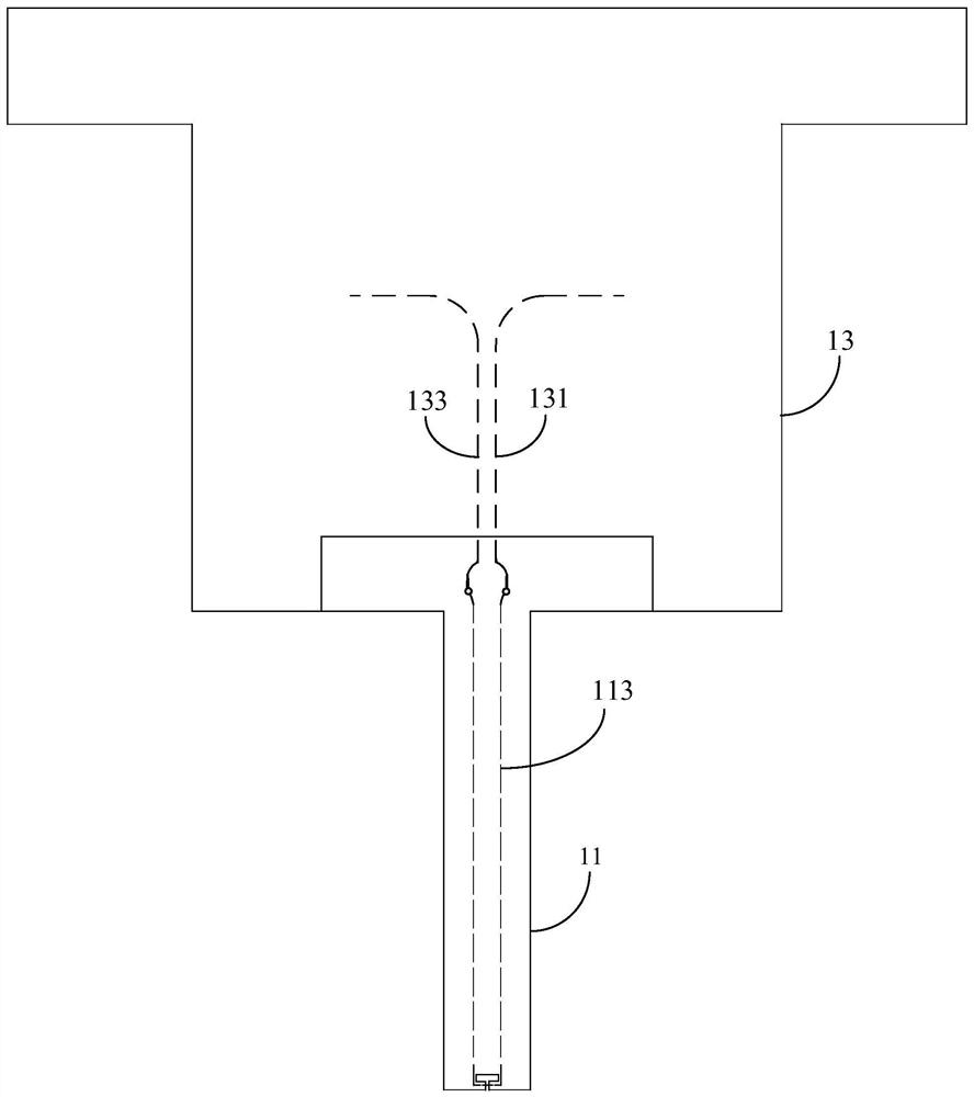
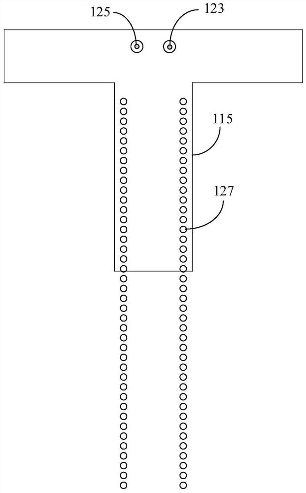
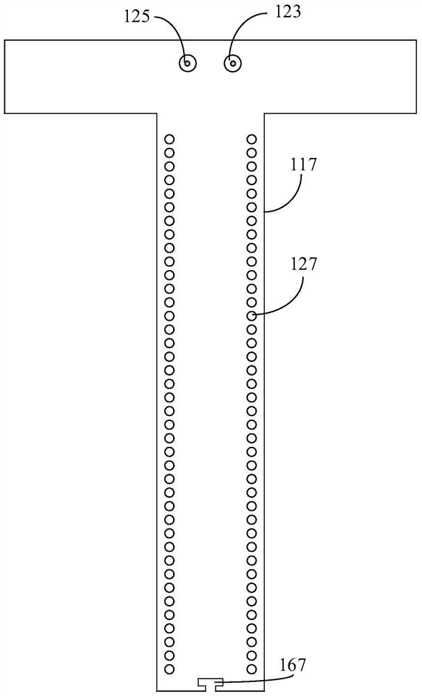
[0047] In order to facilitate the understanding of the present application, the present application will be described more fully below with reference to the relevant drawings. A preferred embodiment of the application is shown in the drawings. However, the present application can be embodied in many different forms and is not limited to the embodiments described herein. On the contrary, the purpose of providing these embodiments is to make the disclosure of this application more thorough and comprehensive.

[0048] It should be noted that when an element is considered to be "connected" to another element, it may be directly connected to and integrally integrated with the other element, or there may be an intervening element at the same time. The terms "carrier", "one end", "other end" and similar expressions are used herein for the purpose of description only.

[0049] Unless otherwise defined, all technical and scientific terms used herein have the same meaning as commonly un...


PUM


Abstract

The application relates to a near-field probe and a near-field detection system; the near-field probe includes a flexible detection part and a circuit carrier; the flexible detection part is mechanically connected to the circuit carrier; wherein, the flexible detection part has a built-in near-field detection line for Electric signals are generated by inductive near-field; the circuit carrier board is built with a first signal transmission line and a second signal transmission line electrically connected to the near-field detection line, which are used to transmit the electrical signal to the network analyzer. The near-field probe of this application adopts a flexible structure The flexible detection part, the thickness of the flexible detection part can be very small, thus providing the spatial resolution of the near-field probe.

Description

technical field [0001] The present application relates to the technical field of near-field probes, in particular to a near-field probe and a near-field detection system. Background technique [0002] In the early stage of circuit design, due to the electromagnetic radiation of electronic components during normal operation, designers usually have to consider the electromagnetic radiation and level of electronic systems. For example, the on-chip current loop is an important radiation source on the integrated circuit, and it will affect other components on the circuit board The normal operation of chips and electronic devices will inevitably be affected. In recent years, with the rapid development of digital circuits and analog circuits and the continuous improvement of operating frequency, it has become more and more important to locate and evaluate electromagnetic interference sources for electronic components, PCB (Printed Circuit Board, printed circuit board) boards, and i...

Claims


Application Information

Patent Timeline
Patent Type & Authority Patents(China)
IPC IPC(8): G01R29/08
CPCG01R29/0871G01R29/0878
Inventor 邵伟恒方文啸黄云恩云飞肖美珍王磊
Owner CHINA ELECTRONICS PROD RELIABILITY & ENVIRONMENTAL TESTING RES INST
Why Eureka
Try Eureka