
Epitaxial wafer silicon slag scraping device for LED lamp production

A technology for LED lamps and scraping devices, which is applied to electrical components, circuits, semiconductor devices, etc., can solve problems such as low work efficiency, reduced actual quality, and inability to achieve continuous processing of batch epitaxial wafers, and achieves high work efficiency and overall structure. compact effect

Pending Publication Date: 2020-04-21
TIANJIN TIANXING ELECTRONICS
View PDF1 Cites 0 Cited by
  • Summary
  • Abstract
  • Description
  • Claims
  • Application Information

AI Technical Summary

Problems solved by technology

Silicon slag will grow on the existing epitaxial wafer, which will affect the subsequent production of LED lamps and reduce its actual quality. Therefore, it is necessary to scrape off the silicon slag
In order to realize the scraping of silicon slag on the epitaxial wafer, the application date is 2017.05.03, the publication number is CN106971940A, and the patent titled "An epitaxial wafer silicon slag scraping device for the production of LED lamps" discloses a A device for scraping and treating silicon slag on the surface of epitaxial wafers, but this device cannot realize continuous processing of epitaxial wafers in batches, and the work efficiency is low. Therefore, in order to meet actual production needs, our company has developed a silicon slag scraping device The corresponding research and development

Method used


Image

  • Epitaxial wafer silicon slag scraping device for LED lamp production
  • Epitaxial wafer silicon slag scraping device for LED lamp production
  • Epitaxial wafer silicon slag scraping device for LED lamp production

Examples


Embodiment 1

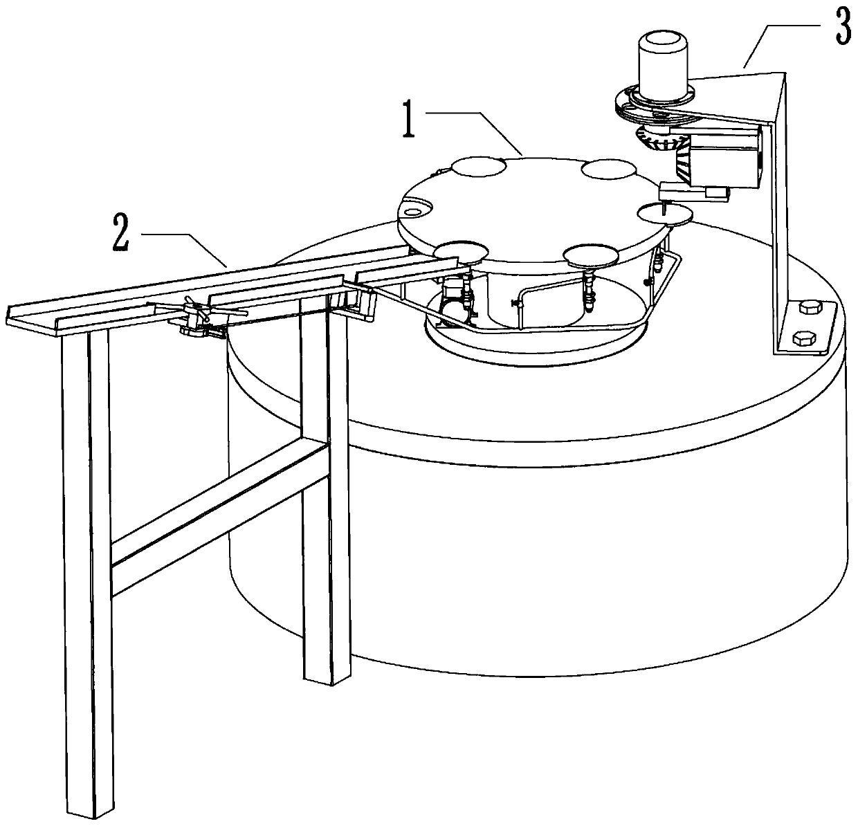
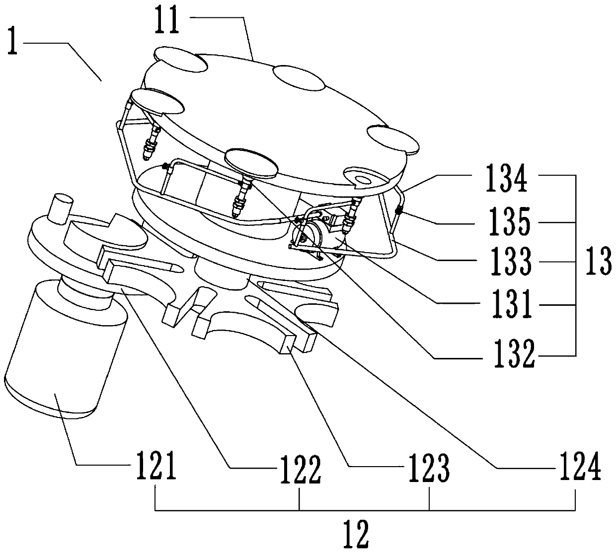
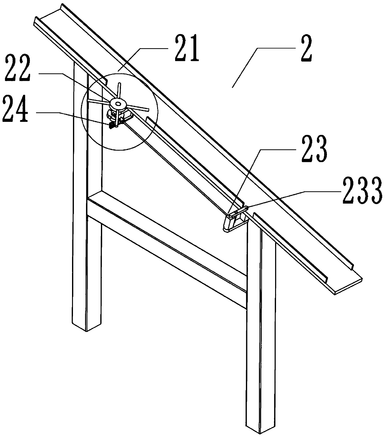
[0044]Such as figure 1 As shown, a silicon slag scraping device for epitaxial wafers used in the production of LED lamps includes a multi-station workbench 1, a feeding mechanism 2 and a slag scraping mechanism 3, and a feeding mechanism is set on the side of the multi-station workbench 1 2 and the slag scraping mechanism 3, and the multi-station workbench 1 rotates intermittently, the feeding mechanism 2 performs a single feeding of the epitaxial wafer to be scraped, and the slag scraping mechanism 3 rotates and scrapes the slag epitaxial sheet to be scraped, and passes through the multi-station The cooperation of the workbench 1, the feeding mechanism 2 and the slag scraping mechanism 3 can carry out continuous single feeding of the epitaxial wafers to be scraped, and the rotation of the slag scraping mechanism 3 ensures the removal of excess silicon slag on the surface of the existing epitaxial wafers. Good scraping, compact overall structure, high working efficiency.

[0...

Embodiment 2

[0066] Such as Figure 7 As shown, the difference from Embodiment 1 is that, further, an epitaxial wafer slag removal mechanism 4 is arranged beside the slag scraping mechanism 3, and the epitaxial wafer slag removal mechanism 4 cleans the silicon slag on the surface of the epitaxial wafer after the slag scraping, Reduce the impact of silicon slag on the surface of epitaxial wafers such as scratches.

[0067] Further, the epitaxial wafer slag removal mechanism 4 is set to include a support frame 2 41, a staggered transmission assembly 2 42, a linear movement assembly 2 43 and a brush 2 44, and the support frame 2 41 is arranged on the side of the multi-station workbench 1, And the support frame 2 41 is provided with a staggered transmission component 2 42 and a linear movement component 2 43 , the staggered transmission component 2 42 drives the linear movement component 43 to move in a straight line, and the output end of the linear movement component 43 is connected to the b...

Embodiment 3

[0073] Such as Figure 8 As shown, the difference from Embodiment 1 and Embodiment 2 is that, further, a lower feeding conveying mechanism 5 is arranged on the side of the epitaxial wafer slag removal mechanism 4, and the setting of the lower feeding conveying mechanism 5 further improves the performance of the scraping device. The automation performance facilitates the unloading of epitaxial wafers after scraping slag on the multi-station workbench 1.

[0074] Further, the blanking conveying mechanism 5 is set to include a conveyor 51 and a blanking frame 52, the conveyor 51 is arranged on the side of the multi-station workbench 1, and the end of the conveyor 51 is provided with a blanking frame 52, and the blanking frame 52 is arranged at the end of the conveyor 51. The end of the rack 52 extends above the conveying line of the next process, and the epitaxial wafer scraped at the station is unloaded and transported by the conveyor 51, and it is conveniently collected in the ...


PUM


Abstract

The invention provides an epitaxial wafer silicon slag scraping device for LED lamp production. The silicon slag scraping device comprises a multi-station workbench, a feeding mechanism and a slag scraping mechanism. The feeding mechanism and the slag scraping mechanism are arranged beside the multi-station workbench. The multi-station workbench intermittently rotates; the feeding mechanism is used for singly feeding an epitaxial wafer which is about to be subjected to slag scraping; and the slag scraping mechanism is used for rotatably scraping slag from the epitaxial wafer which is about tobe subjected to slag scraping. By the adoption of the scraping device, continuous single feeding of the epitaxial wafer which is about to be subjected to slag scraping can be performed, rotary slag scraping can be performed, the scraping device is suitable for well scraping redundant silicon slags on the surface of an existing epitaxial wafer, an overall structure is compact, and working efficiency is high.

Description

technical field [0001] The invention relates to the technical field of epitaxial wafer auxiliary production equipment, in particular to an epitaxial wafer silicon slag scraping device used in the production of LED lamps. Background technique [0002] Silicon epitaxy is to grow one or more layers of silicon single crystal film on a polished silicon single wafer through gas phase chemical reaction at high temperature. By controlling the growth conditions, epitaxial layers with different resistivities, different thicknesses and different types can be obtained. Mainly It is used as an important basic material in the manufacture of various silicon integrated circuits and discrete devices. Silicon slag will grow on the existing epitaxial wafer, which will affect the subsequent production of LED lamps and reduce its actual quality. Therefore, it is necessary to scrape off the silicon slag. In order to realize the scraping of silicon slag on the epitaxial wafer, the application dat...

Claims


Application Information

Patent Timeline
IPC IPC(8): H01L33/00H01L21/02H01L21/67
CPCH01L21/02057H01L21/02096H01L21/67092H01L21/67196H01L33/005
Inventor 李晓辉曹锡文石海莲郭艳艳王红王蔚
Owner TIANJIN TIANXING ELECTRONICS
Learn More