Grid-anode interdigital grid-controlled panel X-ray source and preparation method thereof

An X-ray and anode technology, applied in the direction of X-ray tubes, X-ray tube electrodes, X-ray tube components, etc., to achieve the possible effects of increasing the anode voltage, reducing the fringe electric field, and reducing the occurrence of discharge phenomena

Active Publication Date: 2020-04-24
SUN YAT SEN UNIV
View PDF7 Cites 2 Cited by
  • Summary
  • Abstract
  • Description
  • Claims
  • Application Information

AI Technical Summary

Problems solved by technology

However, the nano-cold cathode electron source array cannot avoid the overlap between the grid electrode and the anode electrode in the application of the flat X-ray source, so there is a serious hidden danger of discharge.

Method used


Image

  • Grid-anode interdigital grid-controlled panel X-ray source and preparation method thereof
  • Grid-anode interdigital grid-controlled panel X-ray source and preparation method thereof
  • Grid-anode interdigital grid-controlled panel X-ray source and preparation method thereof

Examples


Embodiment 1

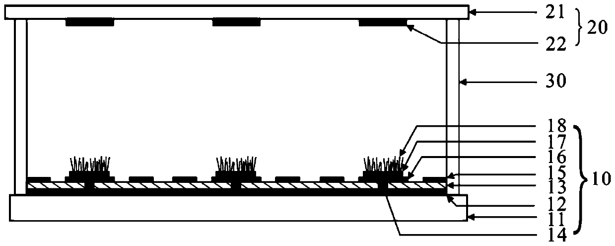
[0048] Such as figure 1 Shown is a schematic structural view of a grid-anode interdigitated grid-controlled flat panel X-ray source of the present invention.

[0049] The nano-cold cathode flat X-ray source of the present invention includes a cathode substrate 10 , an anode substrate 20 , and a high-voltage insulating spacer 30 . The cathode substrate 10 and the anode substrate 20 are arranged parallel to each other, and the high-voltage insulating spacer 30 is arranged between the cathode substrate 10 and the anode substrate 20 to separate and fix the cathode substrate 10 and the anode substrate 20 . There is a certain distance between the cathode substrate 10 and the anode substrate 20 .

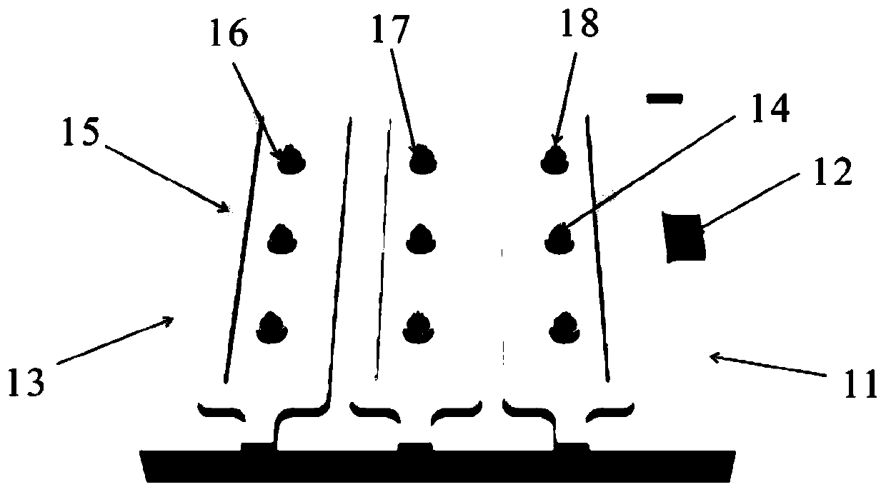
[0050] The cathode substrate 10 includes a cathode substrate 11, a bottom cathode electrode 12 disposed on the cathode substrate 11, an insulating layer 13, an etched through hole 14, a top gate electrode 15, a top cathode electrode 16, and a growth source film 17 and nanowire cold catho...

Embodiment 2

[0073] A fabrication method of a grid-anode interdigitated grid-controlled flat panel X-ray source is basically the same as that of Embodiment 1, the difference being that

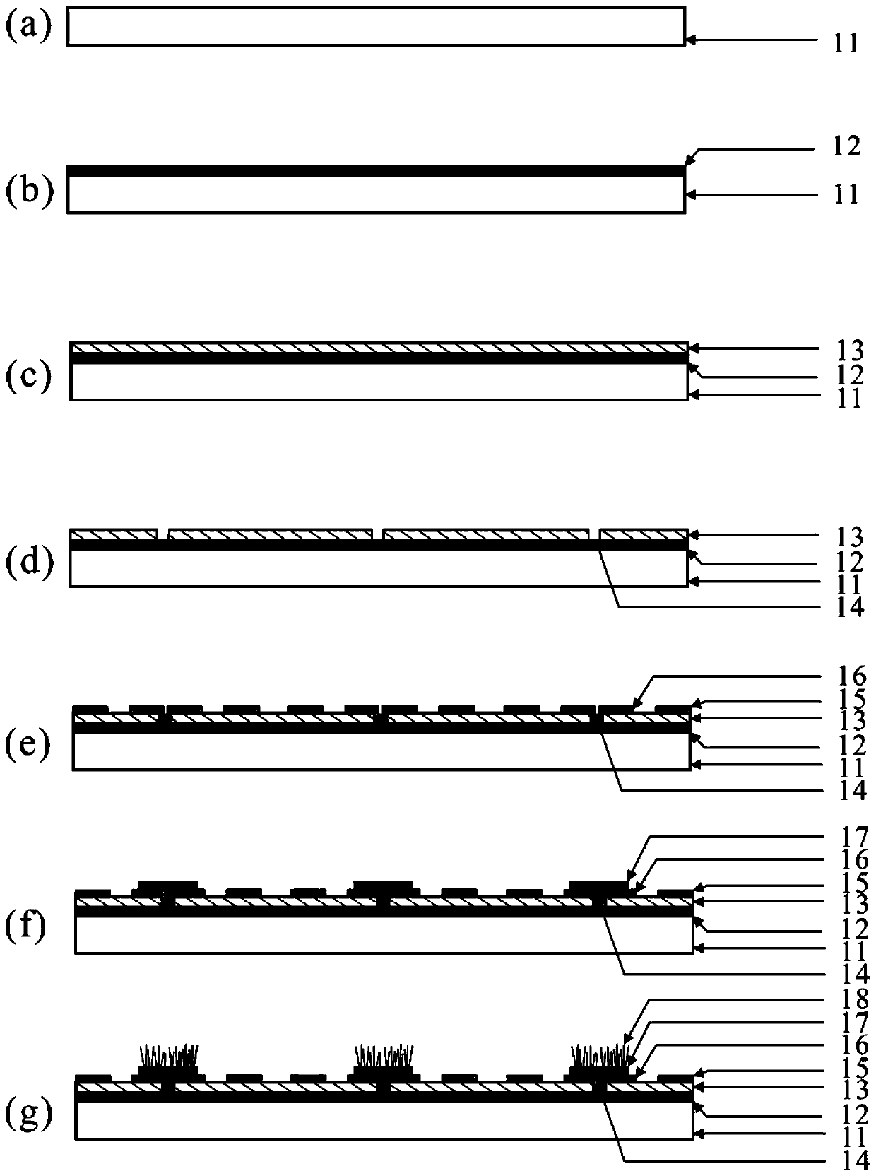
[0074] The cathode substrate 10 is produced.

[0075] (1) The cathode substrate 11 is a large-area silicon wafer.

[0076] (2) The bottom cathode electrode 12 is Cr. The thickness of the bottom cathode electrode 12 is 0.1 μm,

[0077] (3) The insulating film as the insulating layer 13 is composed of a silicon nitride insulating film; the thickness of the insulating layer is 1 μm;

[0078] (4) The top grid electrode 15 and the top cathode electrode 16 are made of Cr, both of which have a thickness of 0.1 μm; their shape is “U”.

[0079](5) On the top cathode electrode 16, photolithography locates the nanowire cold cathode 18 growth region, and then deposits the growth source film 17; the growth source film 17 is copper, and its thickness is 0.3 μm; the diameter of the growth source film is 5 μm, and the...

Embodiment 3

[0087] A fabrication method of a grid-anode interdigitated grid-controlled flat panel X-ray source is basically the same as that of Embodiment 1, the difference being that

[0088] The cathode substrate 10 is produced.

[0089] (1) The cathode substrate 11 is large-area glass.

[0090] (2) The bottom cathode electrode 12 is Ti. The thickness of the bottom cathode electrode 12 is 2 μm,

[0091] (3) The insulating film as the insulating layer 13 is composed of an aluminum oxide insulating film; the thickness of the insulating layer is 5 μm;

[0092] (4) The top gate electrode 15 and the top cathode electrode 16 are made of Ti with a thickness of 2 μm; their shape is "V".

[0093] (5) The growth source film 17 is made of titanium with a thickness of 5 μm; the diameter of the growth source film is 500 μm, and the distance between adjacent growth source films 17 is 50 μm.

[0094] (6) The thermal oxidation growth process is carried out in a box furnace, the heating rate of the ...


PUM

PropertyMeasurementUnit
Thicknessaaaaaaaaaa
Thicknessaaaaaaaaaa
Thicknessaaaaaaaaaa

Abstract

The invention discloses a grid-anode interdigital grid-controlled panel X-ray source, which comprises a cathode substrate, an anode substrate and a high-voltage insulation isolator, wherein the cathode substrate and the anode substrate are oppositely arranged in parallel, and the high-voltage insulation isolator is arranged between the cathode substrate and the anode substrate to isolate the cathode substrate from the anode substrate. The invention further discloses a preparation method of the grid-anode interdigital grid-controlled panel X-ray source, which comprises the steps of manufacturing a cathode substrate, manufacturing an anode substrate and assembling the cathode substrate and the anode substrate. The interdigital arrangement between the grid and the anode can effectively reducethe edge electric field of the top grid electrode, reduce the discharge problem and improve the working stability of the device, so that the anode voltage is further improved while control by the grid realized. Meanwhile, the structure can realize the row addressing function through the control of different grids.

Description

technical field [0001] The invention relates to the technical field of vacuum microelectronic devices, in particular to a grid-anode interdigitated grid-controlled flat-panel X-ray source and a preparation method thereof. Background technique [0002] Chinese patent CN201610542509.8 "Nano-cold cathode electron source array with self-aligning focusing structure and its manufacturing method" etches through holes, and connects the top grid electrode, the top cathode electrode and the bottom cathode electrode strip arranged in parallel with the bottom. The bottom gate electrodes are connected to each other, which solves the problem of complex electrode lead arrangement in the device while realizing gate-controlled row addressing. However, the nano-cold cathode electron source array cannot avoid the overlap between the grid electrode and the anode electrode in the application of the flat X-ray source, so there is a serious hidden danger of discharge. Contents of the invention ...

Claims


Application Information

Patent Timeline
IPC IPC(8): H01J35/04H01J35/06H01J35/08H01J9/00
CPCH01J35/045H01J35/065H01J35/08H01J9/00
Inventor 陈军黄佳邓少芝许宁生佘峻聪
Owner SUN YAT SEN UNIV
Why Eureka
Try Eureka