Sputtering apparatus and method for producing semiconductor device with the same

A sputtering device and semiconductor technology, applied in semiconductor/solid-state device manufacturing, sputter coating, electrical components, etc. Substrate short circuit and other issues

Inactive Publication Date: 2003-06-04
NEC CORP
View PDF2 Cites 0 Cited by
  • Summary
  • Abstract
  • Description
  • Claims
  • Application Information

AI Technical Summary

Problems solved by technology

[0013] However, when using the above-mentioned DC magnetron sputtering device to manufacture semiconductor devices as described above, there is a problem that a short circuit will occur between the gate and the substrate, and the required transistor characteristics cannot be obtained.
[0014] The short circuit between the gate and the substrate is due to the drop in the initial withstand voltage of the gate oxide film

Method used


Image

  • Sputtering apparatus and method for producing semiconductor device with the same
  • Sputtering apparatus and method for producing semiconductor device with the same
  • Sputtering apparatus and method for producing semiconductor device with the same

Examples


Embodiment Construction

[0029] As a result of concentrated and continuous experiments and research conducted to solve the above-mentioned problems, it has been shown that the gate oxide film can be prevented from drop in initial withstand voltage.

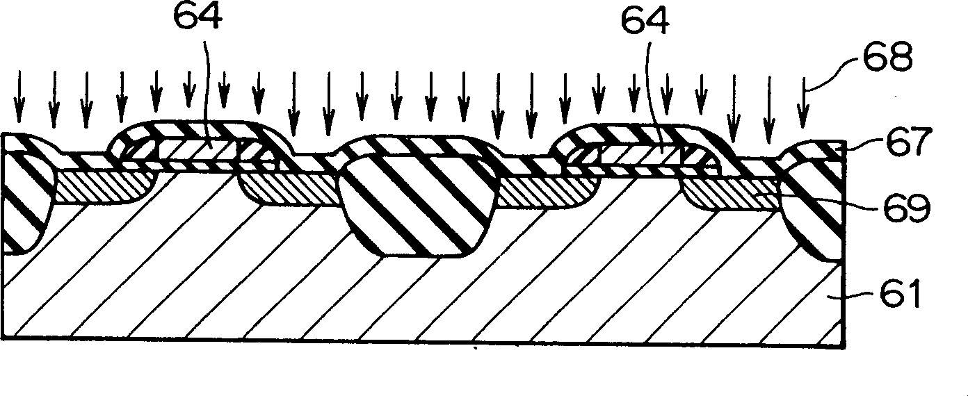
[0030] When a plasma discharge occurs in a conventional DC magnetron sputtering device, the removal of Ar + In addition to ions 97, there are also electrons 99, as shown in Figure 3. Also, in Ar + When the ions 97 collide with the titanium target 83 and bombard the titanium particles 98, a very small amount of electrons 99 are also generated in the plasma. These electrons 99 reach the wafer 86 mounted on the wafer holder 77 in an electrically floating state under the action of the vertical magnetic field generated by the cathode magnet 82 . It is clear that these electrons 99 damage the gate oxide film, resulting in a drop in the initial withstand voltage.

[0031] Damage to the gate oxide film by electrons 99 occurs shortly before the titanium film i...


PUM


Abstract

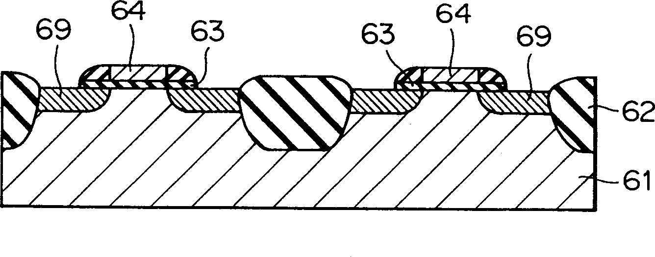
A conductive layer is formed in an area where a gate electrode is to be formed and in an area where a source and drain diffusion layer is to be formed on a semiconductor substrate. Then, a metal film is formed on the conductive layer by sputtering a target for sputtering with a grounded charge trap member provided between the garget and the conductive layer.

Description

technical field [0001] The invention relates to a sputtering device suitable for manufacturing a semiconductor device with a gate oxide film, and a method for manufacturing a semiconductor device with a MOS transistor using the sputtering device, in particular to a sputtering device, and using the sputtering device to manufacture A semiconductor device method for preventing a decrease in the initial withstand voltage of an oxide film. Background technique [0002] In order to increase the operating speed of the element, a method has been adopted in which a refractory metal silicide layer is formed on the surface of the gate electrode and / or the diffusion layer region of the transistor. Specifically, US Pat. No. 4,855,798 discloses a method for forming such a silicide layer in a self-aligned manner. The conventional method of forming a titanium silicide layer as a silicide layer in a self-aligned manner will be described below. 1A to 1G are cross-sectional views illustratin...

Claims


Application Information

Patent Timeline
IPC IPC(8): C23C14/34H01L21/203H01L21/285H01L21/336
CPCC23C14/34H01J37/3447H01L21/2855
Inventor 相泽一雄
Owner NEC CORP
Why Eureka
Try Eureka