Thin film semiconductor device fabrication method and thin film semiconductor device

A technology of thin-film semiconductors and manufacturing methods, which is applied in the manufacture of bottom-gate thin-film semiconductor devices and in the field of thin-film semiconductor devices. It can solve problems such as threshold shift, difficulty in maintaining film quality, and reduced mobility, and achieve fine-scale effects.

Inactive Publication Date: 2011-07-13
SONY CORP +1
View PDF0 Cites 0 Cited by
  • Summary
  • Abstract
  • Description
  • Claims
  • Application Information

AI Technical Summary

Problems solved by technology

[0005] However, if Figure 4 As shown, since the bottom-gate, bottom-contact thin film transistor has a structure in which the source / drain electrodes 109 are disposed on the gate insulating film 107, the steps of forming the source / drain electrodes 109 will affect the gate insulating film 107. s surface
Therefore, for example, when the gate insulating film 107 is made of an organic material, the gate insulating film 107 will become exposed to the organic solvent used to remove the resist pattern forming the source / drain electrode 109 pattern, and become Because it is difficult to maintain the film quality of the surface layer forming the interface with the thin film semiconductor layer 111
Furthermore, such degradation of the interface between the gate insulating film 107 and the thin film semiconductor layer 111 will become a factor causing problems such as threshold shift, mobility drop, etc.

Method used


Image

  • Thin film semiconductor device fabrication method and thin film semiconductor device
  • Thin film semiconductor device fabrication method and thin film semiconductor device
  • Thin film semiconductor device fabrication method and thin film semiconductor device

Examples


no. 1 example

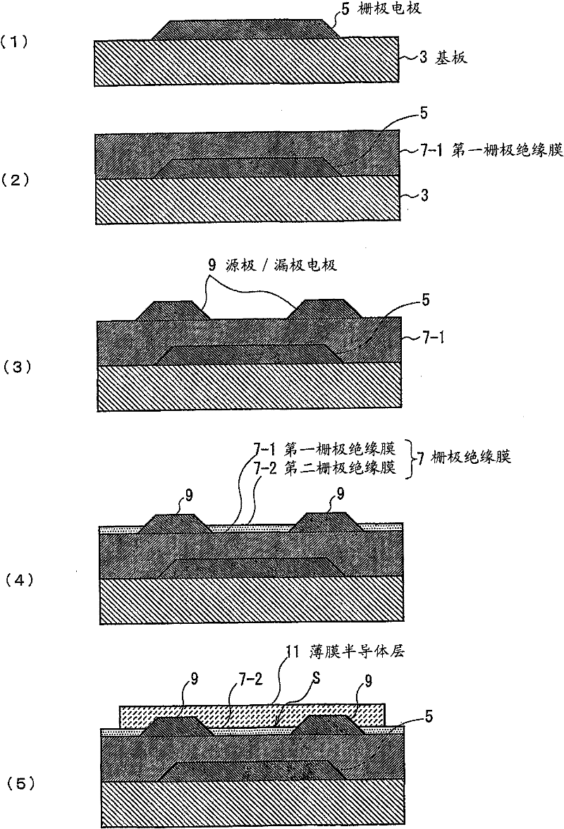
[0017] First, like figure 1 As shown in (1), a substrate 3 is provided. Here, plastic substrates such as polyethylene terephthalate (PET), polyethersulfone (PES), polyethylene naphthalate (PEN), etc., and glass substrates are used. Or stainless steel substrate.

[0018] The gate electrode 5 is formed on the substrate 3. For example, the formation of the gate electrode 5 is performed by forming a metal film and patterning and etching the metal film using a resist pattern formed by photolithography as a mask. The metal film can be formed by a film forming method suitable for the material.

[0019] In the case of metal films such as Al, Cu, Au, Ni, W, Mo, etc., sputtering deposition can be used. In addition, in the case of metal films such as Au, Ag, Ni, Pd, Cr, etc., plating deposition and vapor deposition can be used. Then, after patterning and etching the metal film using the resist pattern as a mask, the resist pattern is removed. The finer gate electrode 5 can be formed usi...

no. 2 example

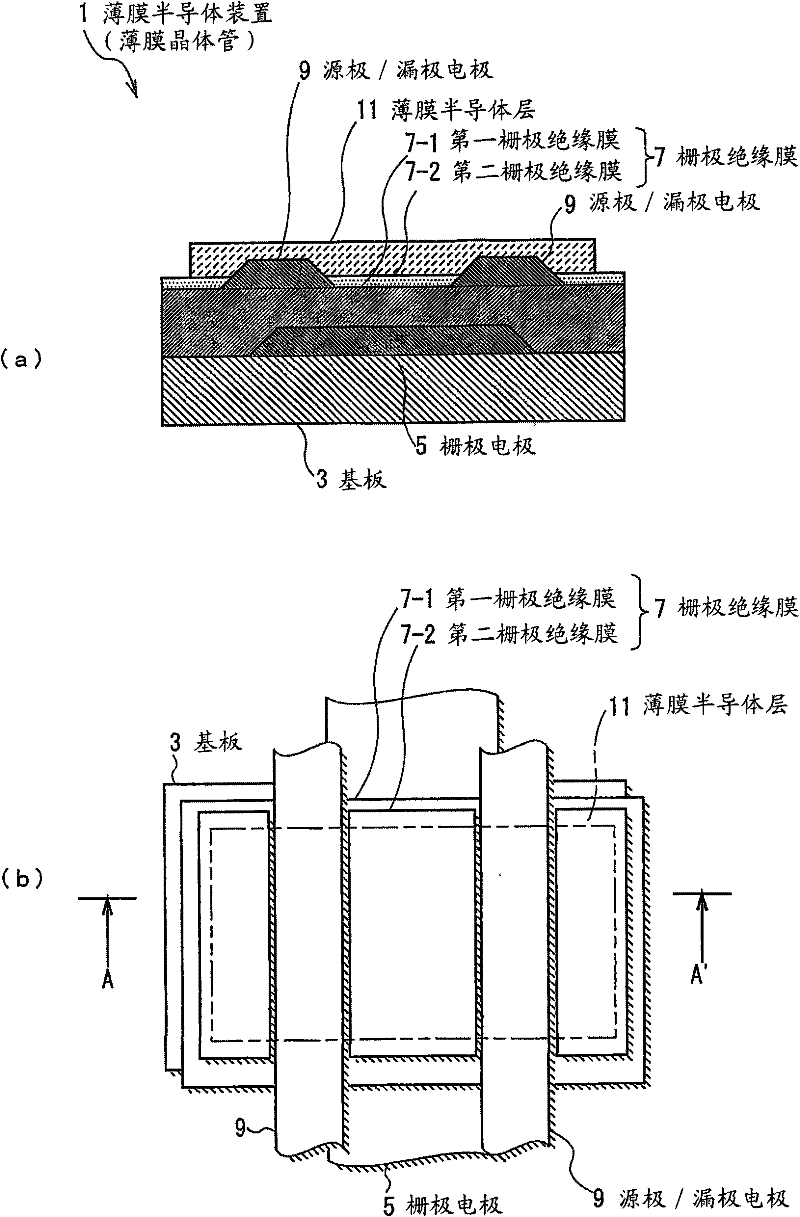
[0038] The second embodiment is that the first gate insulating film 7-1 formed in the first embodiment is changed to include an inorganic insulating film (for example, silicon oxide (SiO x ), silicon nitride (SiN x ) Etc.) and an example of a multilayer structure of an organic insulating film on an inorganic insulating film, and the other structures are the same as in the first embodiment.

[0039] Silicon oxide (SiO) with particularly high stability to gate leakage and electrical current stress x ), silicon nitride (SiN x ) Etc. are preferably used as the inorganic insulating film. The inorganic insulating film is formed by sputtering or plasma enhanced CVD (PECVD: Plasma Enhanced Vapor Chemical Deposition). In addition, the organic material constituting the first gate insulating film 7-1 described in the first embodiment is used as the organic insulating film, and similarly, it is preferable to use a material having particularly high adhesion to the source / drain electrodes 9 Po...

no. 3 example

[0043] The third embodiment is to selectively form the film in the first embodiment through film formation by coating. figure 1 (4) The described method of the second gate insulating film 7-2. Use below figure 1 To describe the manufacturing method of the third embodiment.

[0044] First, as described in the first embodiment, perform figure 1 (1) and figure 1 The step shown in (2) is to form the gate electrode 5 on the substrate 3 and cover the gate electrode 5 with a first gate insulating film 7-1 composed of an organic material. Similarly, polyimide, PVP, poly(α-methylstyrene), etc., which have particularly high adhesion to the source / drain electrodes 9 and have a stable surface state are preferable as the first gate insulating layer. Organic material of film 7-1.

[0045] Then, when figure 1 (3) When forming the source / drain electrode 9 on the first gate insulating film 7-1 in the step shown, use a material that is compatible with the material used to form the second gate ...


PUM


Abstract

Provided is a method for fabricating a bottom gate / bottom contact type thin film semiconductor device (1) which can maintain the boundary between a gate insulation film and a thin film semiconductor layer in a preferable state without being affected by a source / drain electrode and accordingly, can have a preferable characteristic in spite of the fine structure. A first gate insulation film (7-1) is formed in a state to cover a gate electrode (5) formed on a substrate (3). A pair of source / drain electrode (9) is formed on the first gate insulation film (7-1). After this, a second gate insulation film (7-2) is selectively formed only on thefirst insulation film (7-1) exposed from the source / drain electrode (9). Next, a thin film semiconductor layer (11) is formed in contact with the source / drain electrode (9) so as to continuously cover the source / drain electrode (9), the second gate insulation film (7-2), and the first gate insulation film (7-1).

Description

Technical field [0001] The present invention relates to a method for manufacturing a thin film semiconductor device and a thin film semiconductor device, in particular to a method for manufacturing a bottom gate type thin film semiconductor device using an organic semiconductor layer, and the thin film semiconductor device obtained therefrom. Background technique [0002] Thin film transistors are widely used as driving elements in thin electronic substrates, which are particularly active matrix thin display devices. In recent years, semiconductor devices using organic semiconductors as active layers have attracted attention. Since the active layer composed of an organic semiconductor can be formed by low-temperature coating and can be formed on a flexible substrate (for example, plastic, etc.) that does not have thermal resistance, a semiconductor device using an organic semiconductor has an advantage in cost reduction. Not only the active layer, but the gate insulating film, t...

Claims


Application Information

Patent Timeline
Patent Type & Authority Patents(China)
IPC IPC(8): H01L29/786H01L21/336H01L51/05
CPCH01L51/0516H01L51/0529H01L51/001H01L51/0545H10K71/164H10K10/468H10K10/474H10K10/466H10K10/476
Inventor 野本和正平井畅一安田亮一八木岩三成刚生塚越一仁青柳克信
Owner SONY CORP
Why Eureka
Try Eureka