Hybrid probe card applied to silicon-based optoelectronic chip wafer-level online testing

An optoelectronic chip and online testing technology, applied in the field of hybrid probe cards, can solve the problems of limited test chip types, high testing costs, low testing efficiency, etc., to achieve online testing and efficient testing, low testing risk, and improve testing efficiency. Effect

Inactive Publication Date: 2020-05-08
WUHAN POST & TELECOMM RES INST CO LTD +1
View PDF7 Cites 6 Cited by
  • Summary
  • Abstract
  • Description
  • Claims
  • Application Information

AI Technical Summary

Problems solved by technology

[0003] In the process of realizing the present invention, the inventors have found that there are at least the following problems in the prior art: Although silicon-based optoelectronic wafer testing equipment has been released on the market, the equipment needs two motors to control the automatic coupling of two paths of light, and two An additional probe base controls the DC probe and the high-frequency probe respectively, which not only limits the type of test chip, but also has a complex layout, high risk, low test efficiency, and high test cost.

Method used


Image

  • Hybrid probe card applied to silicon-based optoelectronic chip wafer-level online testing
  • Hybrid probe card applied to silicon-based optoelectronic chip wafer-level online testing
  • Hybrid probe card applied to silicon-based optoelectronic chip wafer-level online testing

Examples


Embodiment Construction

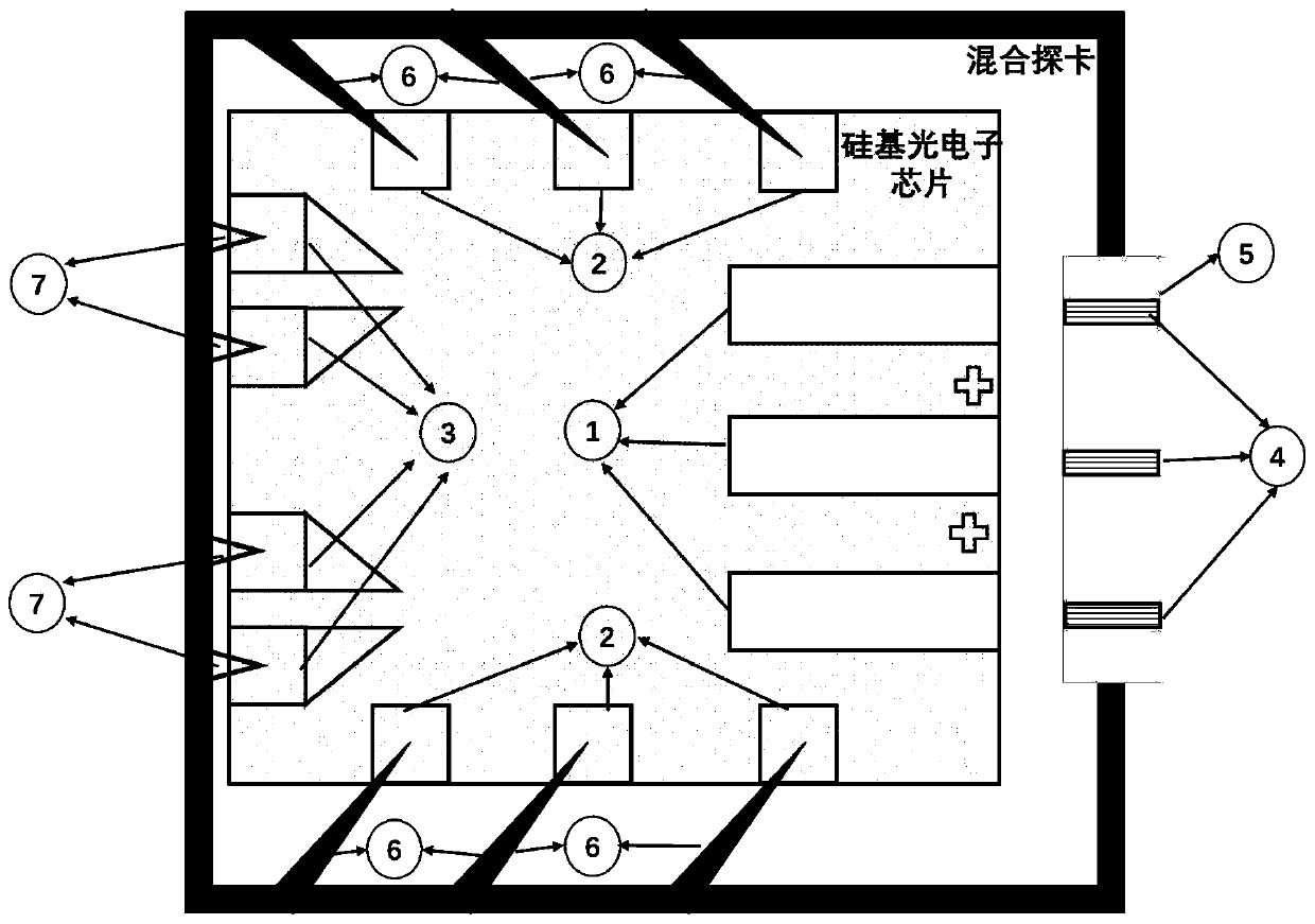
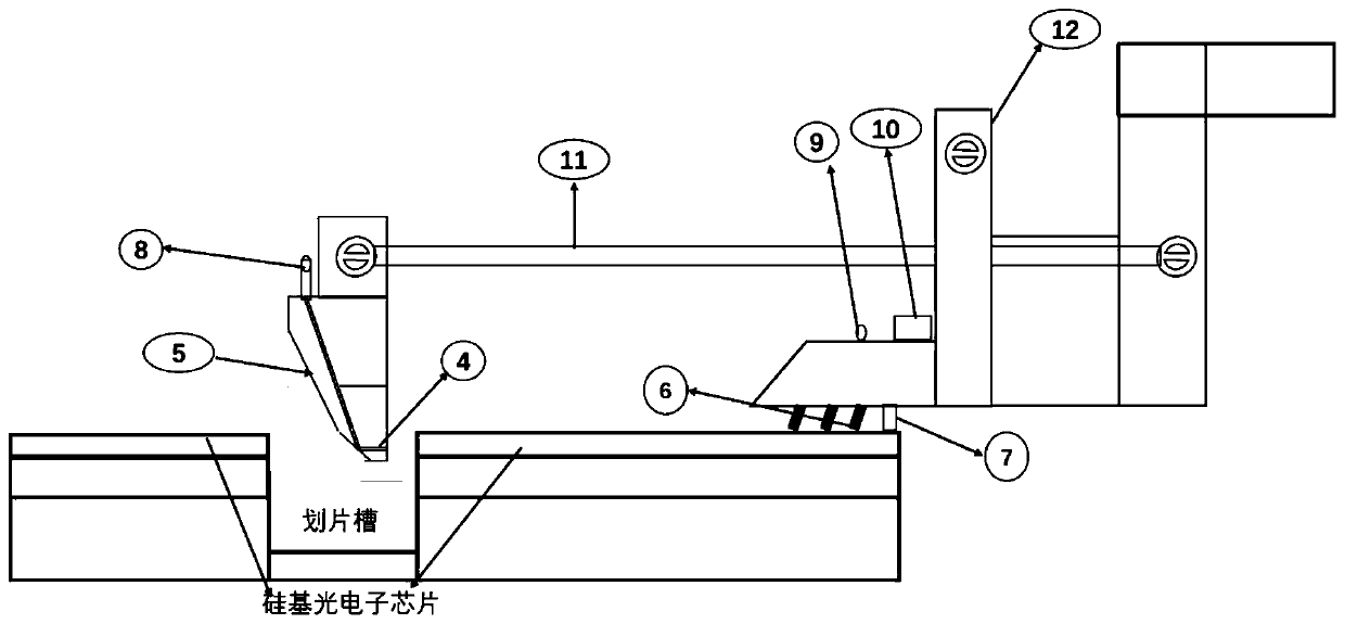
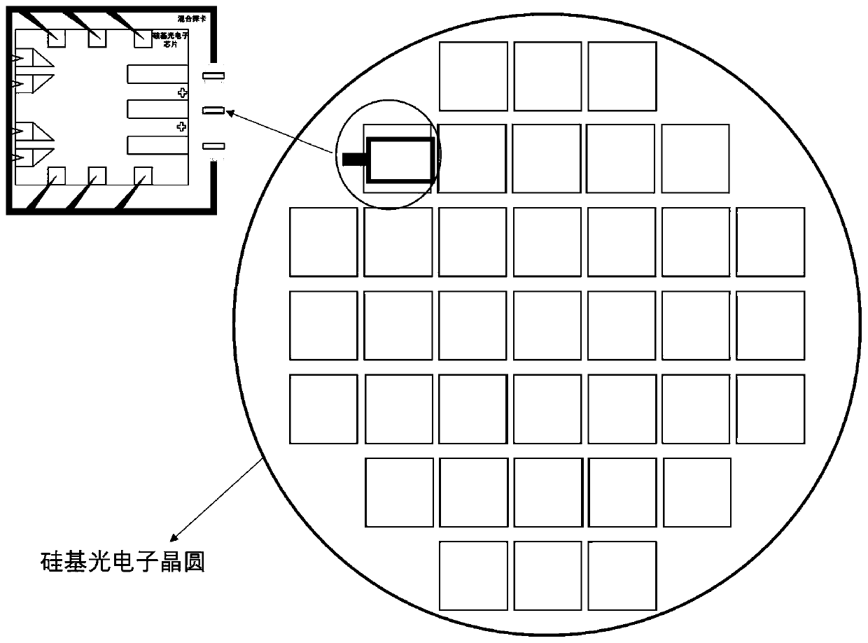
[0021] Reference will now be made in detail to specific embodiments of the invention, examples of which are illustrated in the accompanying drawings. While the invention will be described in conjunction with specific embodiments, it will be understood that it is not intended to limit the invention to the described embodiments. On the contrary, it is intended to cover alterations, modifications and equivalents as included within the spirit and scope of the invention as defined by the appended claims. It should be noted that the method steps described here can all be realized by any functional block or functional arrangement, and any functional block or functional arrangement can be realized as a physical entity or a logical entity, or a combination of both.

[0022] In order to enable those skilled in the art to better understand the present invention, the present invention will be further described in detail below in conjunction with the accompanying drawings and specific embo...


PUM


Abstract

The invention discloses a hybrid probe card applied to silicon-based optoelectronic chip wafer-level online testing, and relates to the field of silicon photon and optoelectronic integration. A hybridprobe card comprises a concave groove array substrate, an optical fiber probe array fixed on the concave groove array substrate, an optical fiber connection port array connected with the optical fiber probe array, an optical fiber probe array control arm used for controlling the optical fiber probe array to move, a direct-current probe array, a direct-current connection port flat cable led out ofthe direct-current probe array, a high-frequency probe array, a high-frequency connection port array led out of the high-frequency probe array, and a direct-current high-frequency probe array controlarm used for controlling the direct-current probe array and the high-frequency probe array to move. According to the invention, the test cost and the test risk of silicon-based photoelectronic chip wafer-level online test can be reduced, the test efficiency is improved, and the method is compatible with the layout of most silicon-based photoelectronic chips.

Description

technical field [0001] The invention relates to the field of integration of silicon photons and optoelectronics, in particular to a hybrid probe card applied to wafer-level on-line testing of silicon-based optoelectronic chips. Background technique [0002] In optoelectronic integrated chips and devices, optoelectronic chip testing involves optical alignment and coupling, which cannot be achieved through an integrated probe card like an electronic chip prepared by a CMOS (Complementary Metal Oxide Semiconductor) process. Level online test. [0003] In the process of realizing the present invention, the inventors have found that there are at least the following problems in the prior art: Although silicon-based optoelectronic wafer testing equipment has been released on the market, the equipment needs two motors to control the automatic coupling of two paths of light, and two An additional probe base controls the DC probe and the high-frequency probe respectively, which not o...

Claims


Application Information

Patent Timeline
Patent Type & Authority Applications(China)
IPC IPC(8): G01R31/28G01R31/311
CPCG01R31/2887G01R31/311
Inventor 冯朋肖希王磊李淼峰
Owner WUHAN POST & TELECOMM RES INST CO LTD
Why Eureka
Try Eureka