Shift register, gate driving circuit, display panel and display device

A shift register and gate technology, which is applied in the field of shift registers, display panels, display devices, and gate drive circuits, and can solve the problems of large leakage current, leakage current, and incomplete closing of transistors in PMOS

Active Publication Date: 2022-04-05
WUHAN TIANMA MICRO ELECTRONICS CO LTD
View PDF7 Cites 0 Cited by
  • Summary
  • Abstract
  • Description
  • Claims
  • Application Information

AI Technical Summary

Problems solved by technology

However, due to the large leakage current of the PMOS formed by Low Temperature Poly-Silicon (LTPS) material, the data update cycle is longer when driving at a low frame rate. When there is a leakage current in the pixel, the display screen may appear Blinking, that is, it cannot be displayed normally
Therefore, some PMOS in the pixel driving circuit can be replaced by NMOS; A "down step", that is, the high level can only be converted to a low level after passing through an intermediate level, so that the high level cannot be effectively shifted, that is, the high potential signal and the low potential signal cannot be realized step by step without loss At the same time, the transistor controlled by the control terminal is not completely closed (that is, "cut off"), and there will still be leakage current, which will affect the display effect

Method used


Image

  • Shift register, gate driving circuit, display panel and display device
  • Shift register, gate driving circuit, display panel and display device
  • Shift register, gate driving circuit, display panel and display device

Examples


Embodiment Construction

[0050] The present invention will be further described in detail below in conjunction with the accompanying drawings and embodiments. It should be understood that the specific embodiments described here are only used to explain the present invention, but not to limit the present invention. In addition, it should be noted that, for the convenience of description, only some structures related to the present invention are shown in the drawings but not all structures.

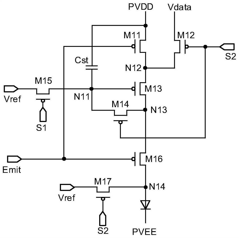
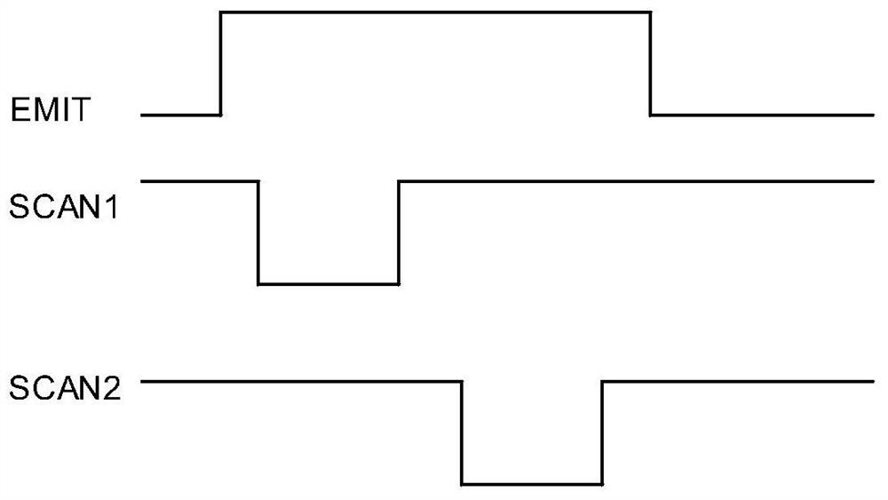
[0051] figure 1 It is a schematic circuit diagram of a pixel driving circuit in the related art, which shows a PMOS designed pixel driving circuit; figure 2 for figure 1 Schematic diagram of driving timing of an exemplary pixel driving circuit, wherein the low-level signal is an enabling signal. refer to figure 1 and figure 2 , the first scanning signal SCAN1 represents the control signal received by the first scanning signal terminal S1, the second scanning signal SCAN2 represents the control signal receive...


PUM


Abstract

The invention discloses a shift register, a gate driving circuit, a display panel and a display device. The shift register includes a second output module and a coupling module, and the two ends of the coupling module are electrically connected to the third node and the second signal output terminal respectively. In the second stage, the potential of the fourth node is the enable potential, and the second output module transmits the high potential signal of the first power signal input terminal to the second output terminal; in the third stage, the potential of the third node is the enable potential , the second output module transmits the low potential signal at the second power supply signal input terminal to the second output terminal, that is, the signal at the second output terminal jumps from high to low; at this time, the low potential signal at the second output terminal is transferred to Coupled to the third node, so that the potential of the third node is lower than that of the second stage, and then the low potential signal at the second power signal input terminal has no transmission loss, which is conducive to completely turning off the transistor controlled by the second signal output terminal, Avoid leakage loss.

Description

technical field [0001] Embodiments of the present invention relate to the field of display technology, and in particular, to a shift register, a gate drive circuit, a display panel, and a display device. Background technique [0002] With the development of display technology, while pursuing a higher resolution of the display device, the power consumption of the display device increases accordingly. In order to reduce power consumption of a display device, a frame rate may be reduced to drive pixels at a low speed during a certain period of time. For example, in a mobile terminal, the normal display mode executes a normal driving frequency based on 60 Hz or 120 Hz; in the standby mode, executes a driving frequency based on 1 Hz-5 Hz, thus reducing power consumption. [0003] Generally, in order to ensure display stability, a pixel driving circuit of a display device may be designed using a P-type metal oxide semiconductor field effect transistor (Positive Channel Metal Oxid...

Claims


Application Information

Patent Timeline
Patent Type & Authority Patents(China)
IPC IPC(8): G11C19/28G09G3/20
CPCG11C19/28G09G3/20G09G2310/0286G09G3/325G09G2310/0243G09G3/3266G09G2330/022G09G2300/0408G09G2310/0289G09G2310/0275G09G3/2092
Inventor 李玥周星耀
Owner WUHAN TIANMA MICRO ELECTRONICS CO LTD
Why Eureka
Try Eureka