
Power increasing method of infrared LED chip made of gallium aluminum arsenic materials

A technology of LED chips and gallium aluminum arsenic, which is applied in the field of power improvement of infrared LED chips, can solve the problems of small light-emitting area and affect the light-emitting power of infrared LED chips, etc. Effect

Active Publication Date: 2020-05-15
深圳市奥伦德元器件有限公司
View PDF8 Cites 4 Cited by
  • Summary
  • Abstract
  • Description
  • Claims
  • Application Information

AI Technical Summary

Problems solved by technology

For the existing infrared LED chip made of gallium aluminum arsenic material, the mixture of nitric acid, glacial acetic acid and water is used to roughen the surface of its P surface, N surface and side surface during the preparation process. Very little, and cannot completely export the light inside the infrared LED chip, which greatly affects the luminous power of the infrared LED chip

Method used


Image

  • Power increasing method of infrared LED chip made of gallium aluminum arsenic materials
  • Power increasing method of infrared LED chip made of gallium aluminum arsenic materials
  • Power increasing method of infrared LED chip made of gallium aluminum arsenic materials

Examples


Embodiment Construction

[0029] Embodiments of the present invention are described in detail below, examples of which are shown in the drawings, wherein the same or similar reference numerals designate the same or similar elements or elements having the same or similar functions throughout. The embodiments described below by referring to the figures are exemplary only for explaining the present invention and should not be construed as limiting the present invention.

[0030] In the description of the present invention, it should be understood that the orientation descriptions, such as up, down, front, back, left, right, etc. indicated orientations or positional relationships are based on the orientations or positional relationships shown in the drawings, and are only In order to facilitate the description of the present invention and simplify the description, it does not indicate or imply that the device or element referred to must have a specific orientation, be constructed and operated in a specific ...


PUM


Abstract

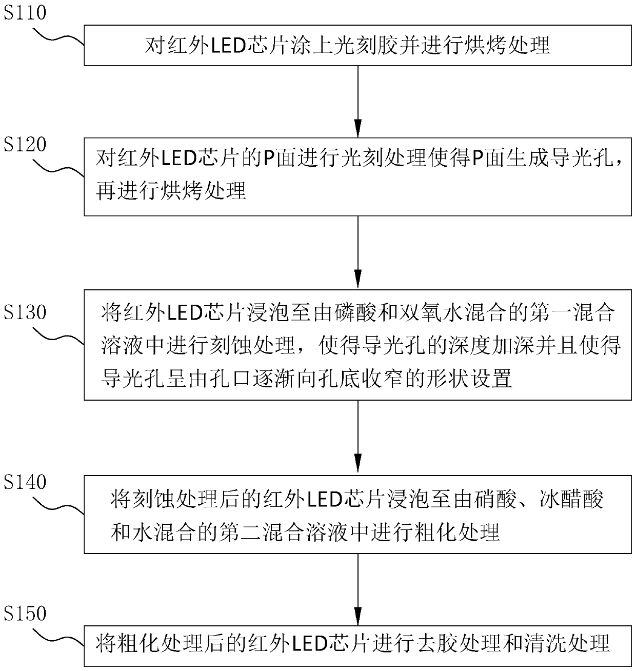
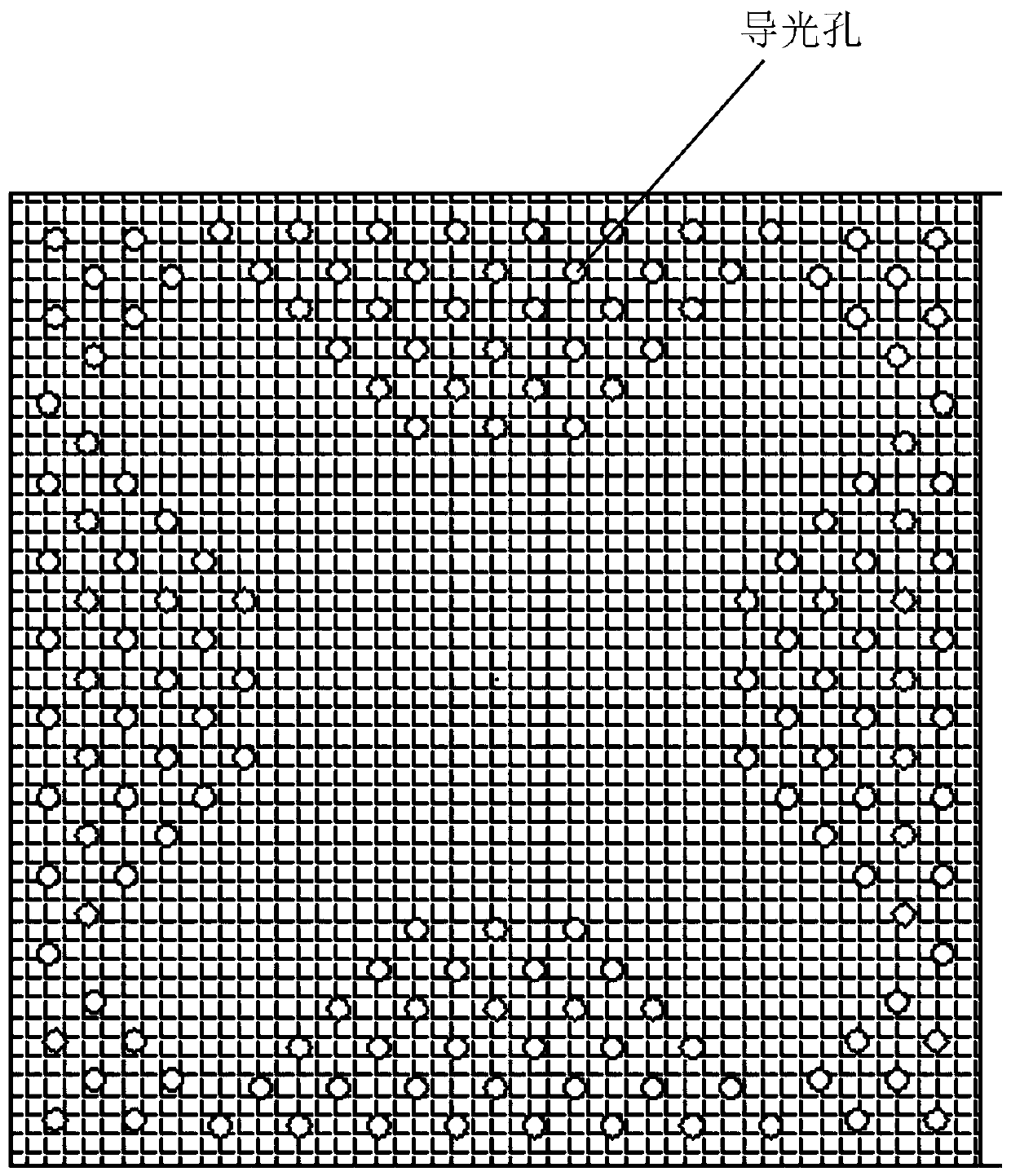
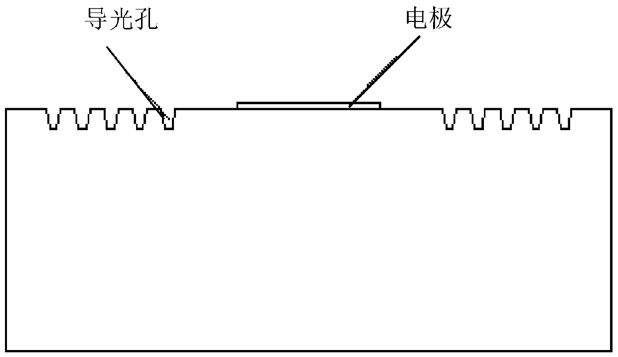
The invention discloses a power increasing method of an infrared LED chip made of gallium aluminum arsenic materials. The method comprises the steps of: coating the infrared LED chip with photoresistand baking the infrared LED chip; carrying out photoetching processing on the P surface of the infrared LED chip to generate a light guide hole in the P surface, and then carrying out baking processing; soaking the infrared LED chip into a first mixed solution formed by mixing phosphoric acid and hydrogen peroxide for etching treatment; soaking the etched infrared LED chip into a second mixed solution formed by mixing nitric acid, glacial acetic acid and water for roughening treatment; and carrying out photoresist removing treatment and cleaning treatment on the infrared LED chip after roughening treatment. The light guide hole is formed in the P surface through photoetching treatment, so that the light-emitting area is increased, and the light-emitting power is improved; the open light guide hole can be formed through etching treatment, so that most of light rays cannot be reflected or absorbed, and the luminous power is improved; in addition, the light-emitting area can be increasedand the light-emitting power can be improved by roughening the surfaces of the P surface, the N surface and the side surface and roughening the light guide hole.

Description

technical field [0001] The invention relates to the technical field of electronic devices, in particular to a method for increasing the power of an infrared LED chip made of gallium aluminum arsenic. Background technique [0002] For infrared LED chips made of gallium aluminum arsenic with a wavelength of 850nm and 940nm, its application range is becoming wider and wider. In the military, it is mainly used in artillery, tanks and individual night vision devices, range finders, stealth monitoring and equipment remote control, etc.; in civilian use, it is mainly used in computer cameras, digital cameras, video cameras, security monitoring, traffic monitoring and home appliance remote controls. With the improvement of people's living standards, the pursuit of long-distance and high-definition is getting higher and higher, so there is an increasing demand for high-power GaAlAs material infrared LED chips. For the existing infrared LED chip made of gallium aluminum arsenic mate...

Claims


Application Information

Patent Timeline
Patent Type & Authority Applications(China)
IPC IPC(8): H01L33/54H01L33/58
CPCH01L33/54H01L33/58H01L2933/0033
Inventor 邱晨吴质朴何畏
Owner 深圳市奥伦德元器件有限公司
Learn More