High density substrate and stacked silicon package assembly having same
A high-density wiring and component technology, applied in the direction of electrical components, semiconductor devices, electrical solid devices, etc., can solve problems such as increased stress levels and device failures
- Summary
- Abstract
- Description
- Claims
- Application Information
AI Technical Summary
Problems solved by technology
Method used
Image

Examples
Embodiment Construction
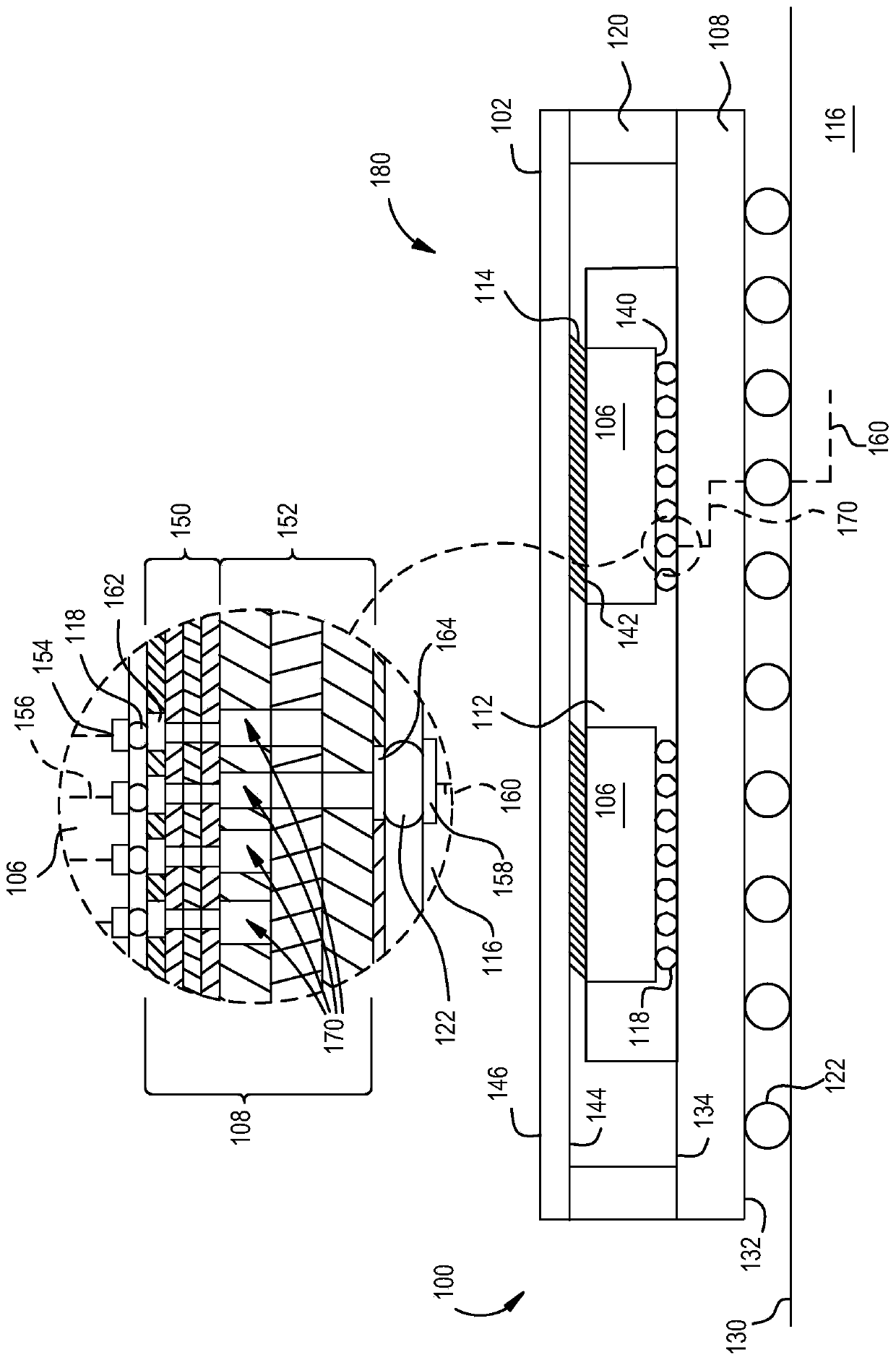
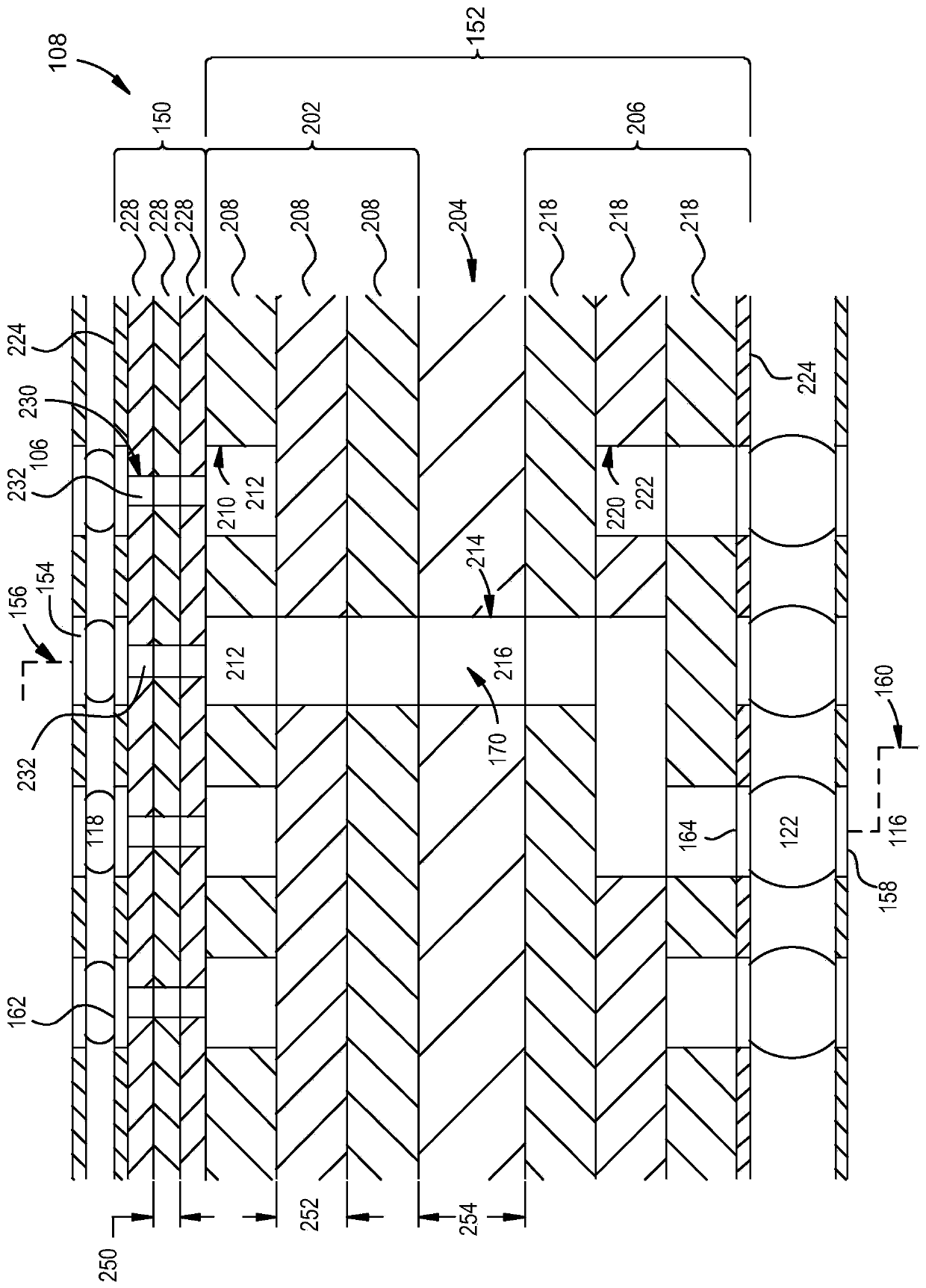
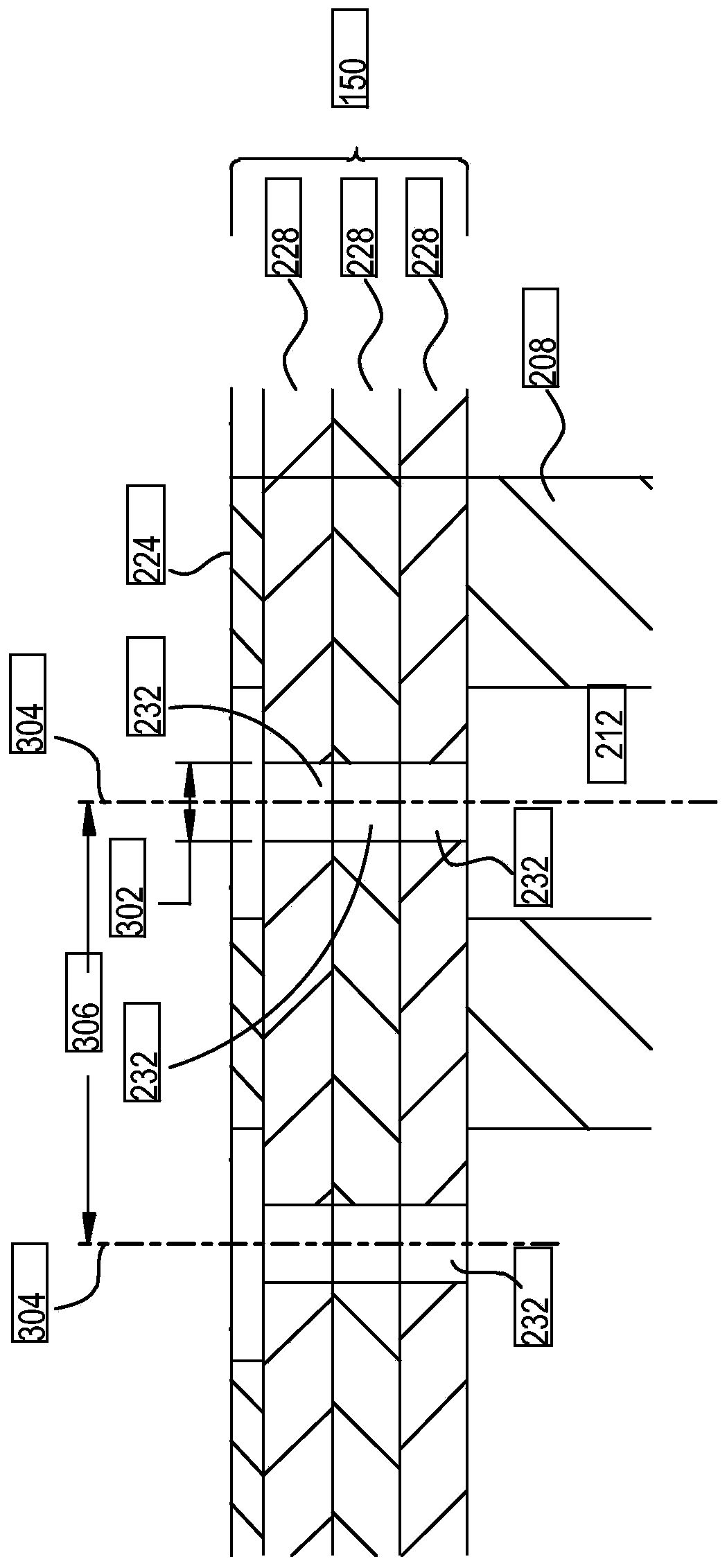
[0018] Provided are an improved interconnection substrate with high-density wiring for a chip package assembly, a chip package assembly with a high-density substrate, and a method of manufacturing the same. The substrate disclosed herein includes a high-density wiring region disposed on a low-density wiring region. High-density routing areas include thinner layers that do not require photoimageable dielectrics and precisely aligned vias, which can greatly reduce stress-induced cracking. In addition, the precise alignment of the vias enables selective solder connections between the substrate and the integrated circuit (IC) die without the use of contact pads, reducing manufacturing cost and Smaller size requirements enable greater wiring density. Further cost savings can be achieved by taking advantage of the reduced density requirements on the printed circuit board side of the substrate, since low density routing areas can be used in the substrate below the high density routi...
PUM
| Property | Measurement | Unit |
|---|---|---|
| Thickness | aaaaa | aaaaa |
Abstract
Description
Claims
Application Information
 - R&D
- Intellectual Property
- Life Sciences
- Materials
- Tech Scout
- Unparalleled Data Quality
- Higher Quality Content
- 60% Fewer Hallucinations
Browse by: Latest US Patents, China's latest patents, Technical Efficacy Thesaurus, Application Domain, Technology Topic, Popular Technical Reports.
© 2025 PatSnap. All rights reserved.Legal|Privacy policy|Modern Slavery Act Transparency Statement|Sitemap|About US| Contact US: help@patsnap.com