Organic electroluminescent device
An electroluminescent device, organic technology, applied in the direction of electric solid devices, electrical components, semiconductor devices, etc., can solve the problems of short brightness decay time and low device efficiency.
- Summary
- Abstract
- Description
- Claims
- Application Information
AI Technical Summary
Problems solved by technology
Method used
Image
Examples
Embodiment 1
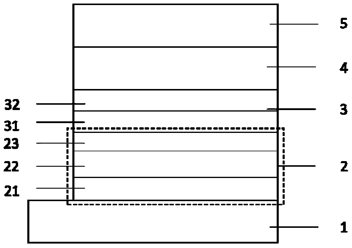
[0155] On an anode glass substrate containing indium tin oxide (ITO) with a film thickness of 150 nm, the vacuum evaporation method is used to achieve a vacuum degree of 2*10 -4 Each film layer was deposited at Pa. First, a HT-a:3%HI-1 thin film was formed on ITO, the ratio of the evaporation rate of HT-a to HI-1 was 1:0.03, the evaporation rate of HT-a was 1 Å / s, and the total thickness was 50nm; then deposit HT-b with a thickness of 90nm, the evaporation rate is 1 Å / s, and then evaporate HT-1 with a thickness of 10nm, the above three-layer film forms the HTL system of this device. Then, the blue host BFH-1 and the dye BFD-1 were co-evaporated from different evaporation sources as the blue light emitting layer. The evaporation rate ratio of the host and the dye was 1:0.05. The thickness of the layer is 5 nm; BFH-1 and YPD-1 are co-evaporated from different evaporation sources as the yellow light emitting layer, and the evaporation rate ratio is 1:0.08, the evaporation rate o...
Embodiment 2
[0158] On an anode glass substrate containing indium tin oxide (ITO) with a film thickness of 150 nm, the vacuum evaporation method is used to achieve a vacuum degree of 2*10 -4 Each film layer was deposited at Pa. First, a HT-a:3%HI-1 film was formed on ITO, the ratio of the evaporation rate of HTA to HI-1 was 1:0.03, the evaporation rate of HT-a was 1 Å / s, and the total thickness was 70 nm; Next, HT-b with a thickness of 70 nm was deposited, and the evaporation rate was 1 Å / s, and then HT-1 with a thickness of 10 nm was deposited. The above three-layer film formed the HTL system of the device. Then, the blue host BFH-1 and the dye BFD-1 were co-evaporated from different evaporation sources as the blue light emitting layer. The evaporation rate ratio of the host and the dye was 1:0.05. The thickness of the layer is 5 nm; BFH-1 and YPD-1 are co-evaporated from different evaporation sources as the yellow light emitting layer, and the evaporation rate ratio is 1:0.08, the evapo...
Embodiment 3
[0161] On an anode glass substrate containing indium tin oxide (ITO) with a film thickness of 150 nm, the vacuum evaporation method is used to achieve a vacuum degree of 2*10 -4 Each film layer was deposited at Pa. First, a HT-a:3%HI-1 thin film was formed on ITO, the ratio of the evaporation rate of HT-a to HI-1 was 1:0.03, the evaporation rate of HT-a was 1 Å / s, and the total thickness was 50nm; then deposit HT-a with a thickness of 90nm, the evaporation rate is 1 Å / sec, and then evaporate HT-1 with a thickness of 10nm, the above three-layer film forms the HTL system of this device. Then, the blue host BFH-1 and the dye BFD-1 were co-evaporated from different evaporation sources as the blue light emitting layer. The evaporation rate ratio of the host and the dye was 1:0.05. The thickness of the layer is 5 nm; BFH-1 and YPD-1 are co-evaporated from different evaporation sources as the yellow light emitting layer, and the evaporation rate ratio is 1:0.08, the evaporation rate...
PUM
| Property | Measurement | Unit |
|---|---|---|
| thickness | aaaaa | aaaaa |
Abstract
Description
Claims
Application Information


