Supercharge Your Innovation With Domain-Expert AI Agents!

Deep ultraviolet LED device with visible light wave band and preparation method of deep ultraviolet LED device

A LED device, deep ultraviolet technology, applied in the direction of semiconductor devices, electrical components, circuits, etc., can solve the problem that deep ultraviolet devices cannot cover the visible light band at the same time, and are difficult to identify, so as to reduce the production cost and simplify the production process.

Active Publication Date: 2020-06-02
SUZHOU UVCANTEK CO LTD
View PDF7 Cites 4 Cited by
  • Summary
  • Abstract
  • Description
  • Claims
  • Application Information

AI Technical Summary

Problems solved by technology

[0003] The purpose of the present invention is to provide a deep ultraviolet LED device with visible light band and its preparation method, which is used to solve the problem that deep ultraviolet devices in the prior art cannot cover the visible light band at the same time, which makes it difficult to identify when working

Method used


Image

  • Deep ultraviolet LED device with visible light wave band and preparation method of deep ultraviolet LED device
  • Deep ultraviolet LED device with visible light wave band and preparation method of deep ultraviolet LED device

Examples


Embodiment Construction

[0018] The following will clearly and completely describe the technical solutions in the embodiments of the present invention with reference to the accompanying drawings in the embodiments of the present invention. Obviously, the described embodiments are only some, not all, embodiments of the present invention. Based on the embodiments of the present invention, all other embodiments obtained by persons of ordinary skill in the art without making creative efforts belong to the protection scope of the present invention.

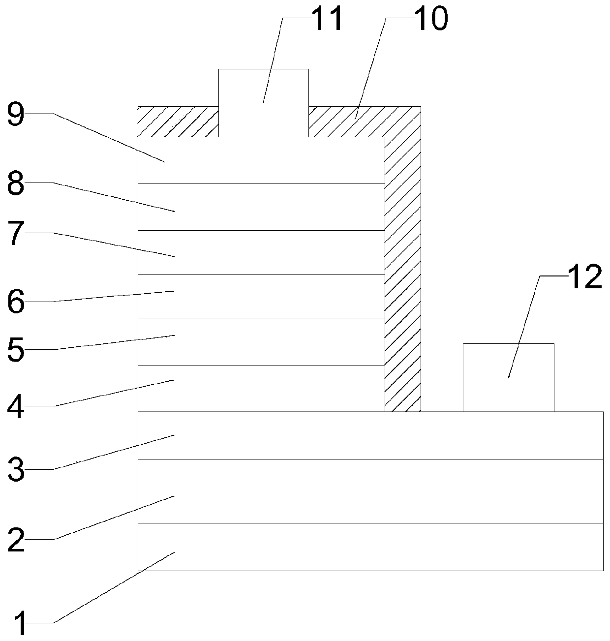
[0019] For the first solution proposed by the present invention, see figure 1 , figure 1 It is a structural schematic diagram of an embodiment of a deep ultraviolet LED device with a visible light band in the present invention. In the present invention, the deep ultraviolet LED device with visible light band is provided with a sapphire substrate 1, an AlN intrinsic layer 2, an n-type AlGaN layer 3, a current spreading layer 4, a deep ultraviolet band quantum ...


PUM

PropertyMeasurementUnit
thicknessaaaaaaaaaa
thicknessaaaaaaaaaa
temperatureaaaaaaaaaa

Abstract

The invention discloses a deep ultraviolet LED device with a visible light waveband and a preparation method of the deep ultraviolet LED device. The deep ultraviolet LED device with the visible lightwave band is sequentially provided with a sapphire substrate, an AlN intrinsic layer, an n-type AlGaN layer, a current expansion layer, a deep ultraviolet band quantum well active layer, a visible band quantum well active layer, an electron blocking layer, a p-type AlGaN injection layer, a p-type GaN contact layer, a DBR layer, a p electrode and an n electrode from bottom to top. According to theinvention, a deep ultraviolet band quantum well based on an AlGaN material and a visible light band quantum well based on an InGaN material are integrated in an epitaxial structure in a monolithic manner; therefore, the single device can emit light in both the deep ultraviolet band and the visible light band, the manufacturing process of a double-color lamp bead device is simplified, and the manufacturing cost of the double-color lamp bead device is reduced.

Description

technical field [0001] The invention relates to the field of semiconductor optoelectronics, in particular to a deep ultraviolet LED device with visible light band and a preparation method thereof. Background technique [0002] At present, group III nitrides, as outstanding representatives of wide bandgap semiconductor materials, have realized high-efficiency blue-green light-emitting diodes (light-emitting diodes, referred to as LEDs), lasers and other solid-state light source devices. and other applications have achieved great success. In the past ten years, people expect to apply this high-efficiency luminescent material to the ultraviolet band to meet the increasing demand for ultraviolet light sources. According to its biological effects, the ultraviolet band can usually be divided into: long-wave ultraviolet (abbreviated as UVA, wavelength range 320-400nm), medium-wave ultraviolet (abbreviated as UVB, wavelength range 280-320nm), short-wave ultraviolet (abbreviated as ...

Claims


Application Information

Patent Timeline
Patent Type & Authority Applications(China)
IPC IPC(8): H01L33/06H01L33/14H01L33/44H01L33/00
CPCH01L33/007H01L33/06H01L33/14H01L33/145H01L33/44H01L2933/0025
Inventor 张骏袁章洁戴江南陈长清
Owner SUZHOU UVCANTEK CO LTD
Features
  • R&D
  • Intellectual Property
  • Life Sciences
  • Materials
  • Tech Scout
  • Unparalleled Data Quality
  • Higher Quality Content
  • 60% Fewer Hallucinations
Learn More