Method for detecting electroneutral defect state of amorphous selenium

A technology of amorphous selenium and defect states, applied in the direction of material excitation analysis, Raman scattering, etc., can solve the problems of unusable detection, only applicable to charged defect states, imperfect detection technology of amorphous selenium, etc., and achieve feasibility high effect

Inactive Publication Date: 2020-06-05
JILIN UNIV
View PDF2 Cites 4 Cited by
  • Summary
  • Abstract
  • Description
  • Claims
  • Application Information

AI Technical Summary

Problems solved by technology

Among them, the steady-state and transient photoconductivity test methods are more successful in studying the defect state density of amorphous selenium, but because this method relies on the test of the photoconductive properties of the material, it is usually more effective in detecting charged defect states, and The good insulating properties of the material caused by the wide band gap (1.95eV) of amorphous selenium at low temperature are not conducive to accurate conductance testing; photoinduced electron spin resonance is also only suitable for charged defect states, not for electrically neutral ones. The detection of defect states, and the detection of electron spin resonance signals need to be carried out in a low-temperature environment; although the resonance Raman scattering technique is an effective method for studying the interband transition of semiconductors, the detection of amorphous selenium defect states by this technology is currently not realized
In summary, the detection technology for various defect states of amorphous selenium, especially for electroneutral defect states, is still incomplete.

Method used


Image

  • Method for detecting electroneutral defect state of amorphous selenium
  • Method for detecting electroneutral defect state of amorphous selenium
  • Method for detecting electroneutral defect state of amorphous selenium

Examples


Embodiment Construction

[0023] The technical solution of the present invention will be specifically described below in conjunction with the accompanying drawings. The invention is a method for detecting the electroneutral defect state of amorphous selenium by using the pressure-induced resonance Raman scattering technology. By accurately measuring the resonance pressure of the first-order and second-order Raman peaks of the tensile vibration mode of amorphous selenium chain molecular bonds, the energy level of the electroneutral defect state caused by the dihedral angle distortion of amorphous selenium and its dependence on pressure can be obtained. The changing relationship, specifically includes the following steps:

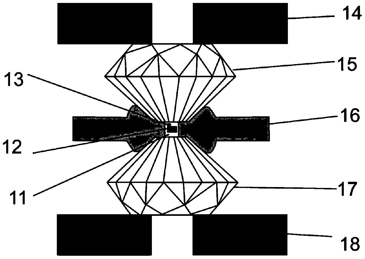
[0024] Step S1: Putting the amorphous selenium sample into the diamond counter-anvil cavity, and applying pressure to the sample;

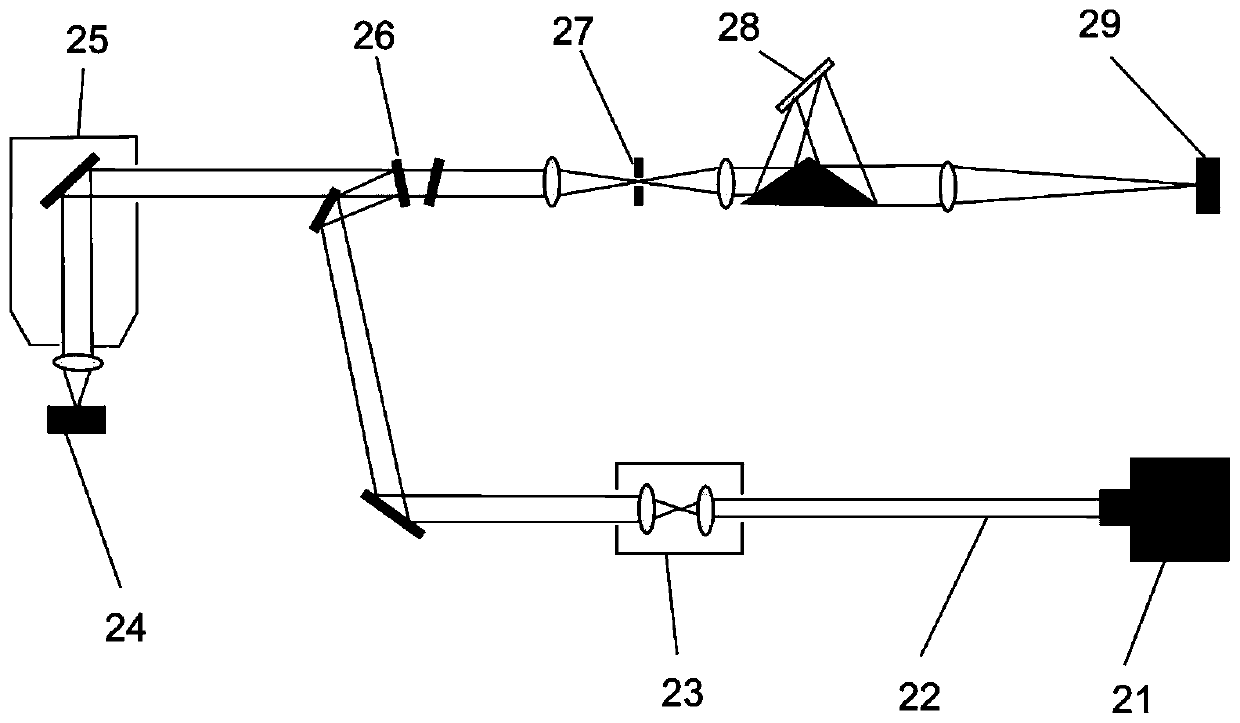
[0025] Step S2: measuring Raman scattering signals of amorphous selenium under different pressures;

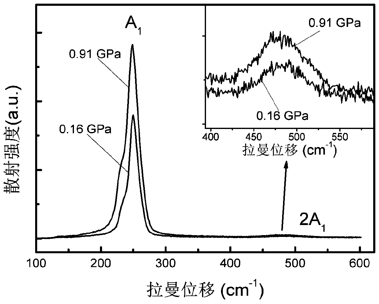
[0026] Step S3: Determining the defect state ener...


PUM


Abstract

The invention relates to a method for detecting the electroneutral defect state of amorphous selenium, which belongs to the field of physical property detection of semiconductor materials, and particularly comprises the following steps: S1, loading an amorphous selenium sample into a diamond anvil cell pressing cavity, and applying pressure to the sample; S2, measuring Raman scattering signals ofamorphous selenium under different pressures; and S3, determining the defect state energy level by analyzing the change of the Raman scattering intensity along with the pressure. The method provided by the invention is high in feasibility, simple and feasible, can effectively detect the electrically neutral defect state of the amorphous selenium caused by dihedral angle distortion, and can accurately determine the defect state energy level and the change relationship of the defect state energy level with the pressure.

Description

technical field [0001] The invention belongs to the field of physical property detection of semiconductor materials, and in particular relates to a method for detecting the electroneutral defect state of amorphous selenium. Background technique [0002] Amorphous selenium is widely used as a semiconductor material, and the research on its semiconductor material properties has always attracted people's attention. Its unique photosensitivity and optoelectronic properties make amorphous selenium have very important application value in various technical applications such as solar cells, photocopying technology, X-ray imaging and digital X-ray radiography. Amorphous selenium has a variety of defect states in the band gap, and the typical ones are intrinsic defects caused by valence conversion with negative correlation energy, coordination defects and dihedral angle distortion. The coordination defects are based on the coordination number The change of will form deep-level defec...

Claims


Application Information

Patent Timeline
Patent Type & Authority Applications(China)
IPC IPC(8): G01N21/65
CPCG01N21/65
Inventor 杨凯锋李恒梅邹广田
Owner JILIN UNIV
Why Eureka
Try Eureka