A conductive film and a patterning method thereof

A conductive film and patterning technology, which is applied to conductive materials, conductive materials, conductive layers on insulating carriers, etc., can solve the problems of copper layer being easily oxidized, conductivity changes, surface resistance and conductivity fluctuations, etc., to achieve suppression Effects of natural oxidation, damage suppression, and etching suppression

Pending Publication Date: 2020-06-05
NITTO DENKO CORP
View PDF2 Cites 1 Cited by
  • Summary
  • Abstract
  • Description
  • Claims
  • Application Information

AI Technical Summary

Problems solved by technology

In such a conductive film with a copper layer, the copper layer is easily oxidized, and the conductivity changes over time. Therefore, over a long period of time, there is a problem that the conductivity such as surface resistance (sheet resistance) fluctuates when viewed from above.

Method used


Image

  • A conductive film and a patterning method thereof
  • A conductive film and a patterning method thereof
  • A conductive film and a patterning method thereof

Examples


Embodiment 1

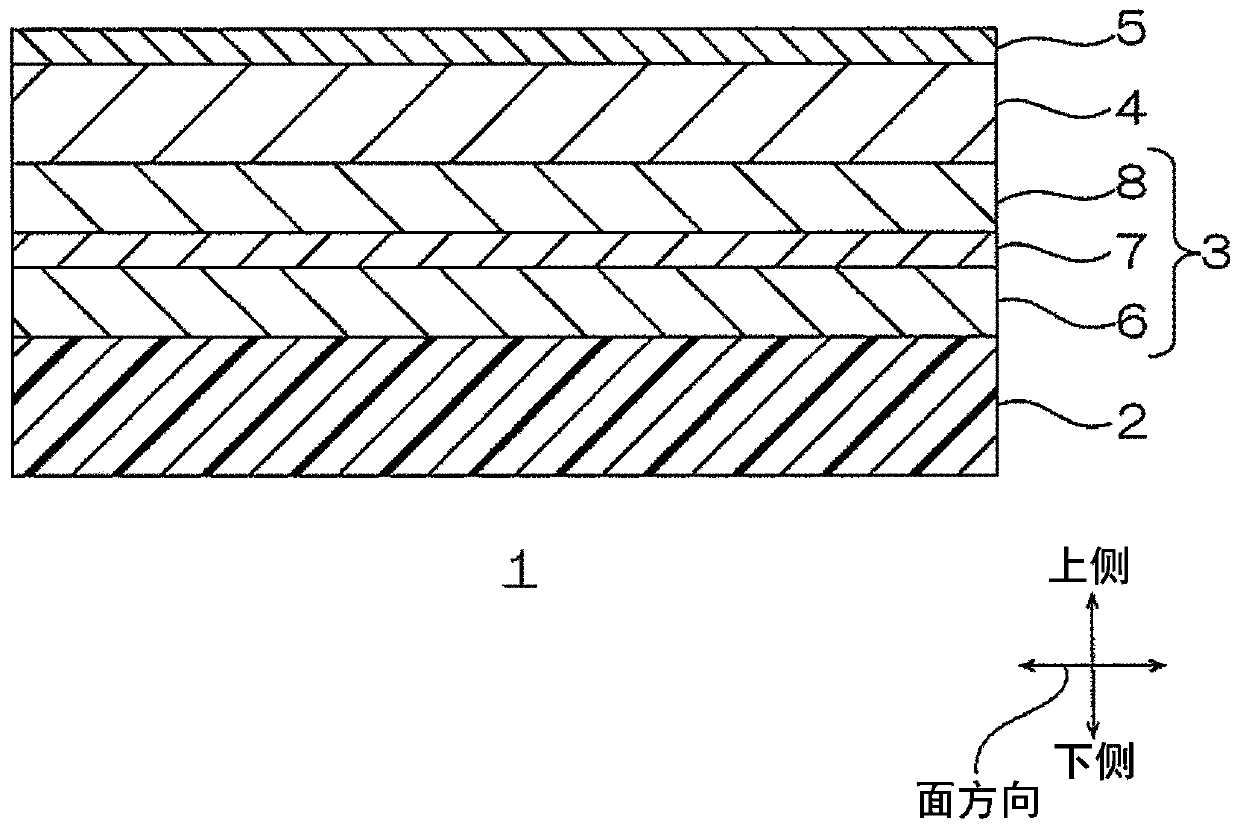
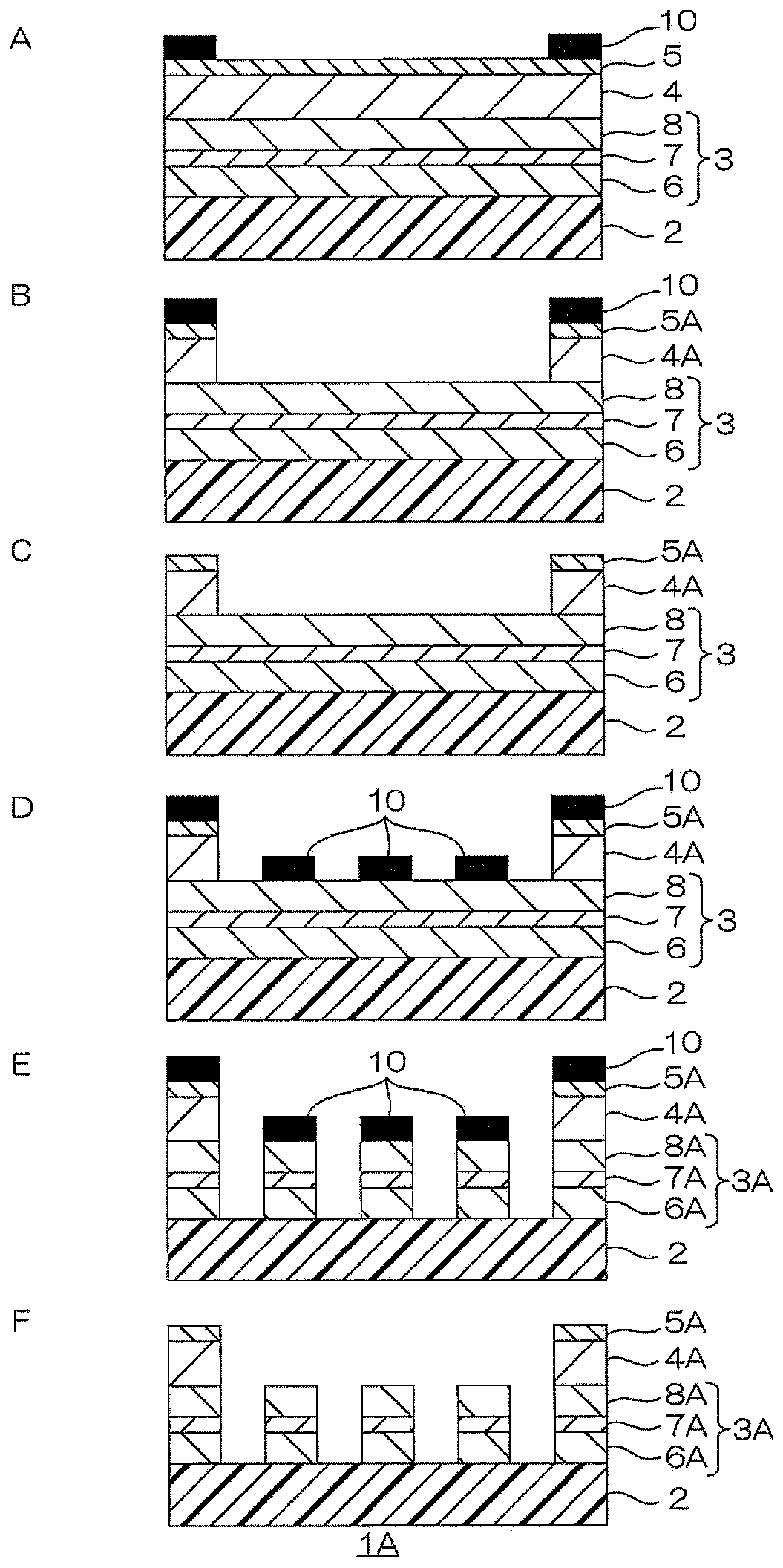
[0156] As a transparent substrate, a polyethylene terephthalate (PET) film with a thickness of 50 μm was prepared.

[0157] Next, the PET film was introduced into a vacuum sputtering device, and an indium tin oxide layer with a thickness of 40 nm, a silver layer with a thickness of 8 nm, and an indium tin oxide layer with a thickness of 36 nm were sequentially formed by sputtering to form a transparent conductive layer.

[0158] In the formation of the indium tin oxide layer, a target made of a sintered body of 12% by mass tin oxide and 88% by mass of indium oxide was used, and a target made of an Ag alloy was used for the formation of the silver layer.

[0159] Next, the PET film on which the transparent conductive layer was laminated was introduced into a vacuum sputtering apparatus, and a copper layer with a thickness of 200 nm was formed by the sputtering method.

[0160] Specifically, the transparent conductive layer was sputtered using a Cu target made of oxygen-free cop...

Embodiment 2~4

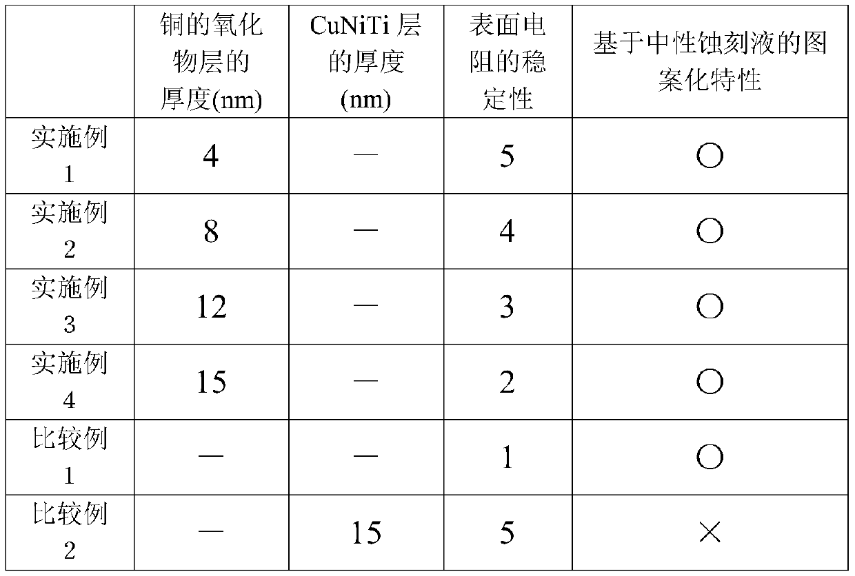
[0165] Except having changed the thickness of the oxide layer of copper into the thickness of Table 1, it carried out similarly to Example 1, and obtained the electroconductive thin film.


PUM

PropertyMeasurementUnit
thicknessaaaaaaaaaa
thicknessaaaaaaaaaa
thicknessaaaaaaaaaa

Abstract

The invention relates to a conductive film and a patterning method thereof. Provided are: a conductive film which has excellent copper layer stability, is capable of easily patterning a copper layer,and is capable of suppressing damage to a metal layer within a transparent conductive layer; and a patterning method therefor. A conductive film (1) is provided with: a transparent substrate (2); a transparent conductive layer (3) that is disposed on the upper side of the transparent substrate (2) and is provided with a first inorganic oxide layer (6), a metal layer (7), and a second inorganic oxide layer (8) in this order; a copper layer (4) disposed on the upper side of the transparent conductive layer (3); and a copper oxide layer (5) disposed on the upper side of the copper layer (4).

Description

technical field [0001] The present invention relates to a conductive film and a method for patterning the same. Specifically, it relates to a conductive film suitable for optical use and a method for patterning the same. Background technique [0002] Conventionally, it is known that a transparent conductive film having a transparent conductive layer is used for optical applications such as a touch panel. [0003] For example, it is described that a transparent conductive film is provided with a transparent substrate and a light-transmitting inorganic layer, and the light-transmitting inorganic layer sequentially includes a first inorganic oxide layer, a metal layer, and a second inorganic oxide layer (for example, refer to Patent Literature 1). [0004] In the transparent conductive film of Patent Document 1, for example, it is known that a metal layer such as a silver layer functions as a conductive layer. Therefore, compared with a conventional transparent conductive laye...

Claims


Application Information

Patent Timeline
Patent Type & Authority Applications(China)
IPC IPC(8): G06F3/041
CPCG06F3/041G06F2203/04103H01B5/14H01B1/026H05K1/0313H05K1/09
Inventor 片山隆平松本圭祐安藤豪彦
Owner NITTO DENKO CORP
Why Eureka
Try Eureka