MOS device with annular channel region and preparation method thereof

A MOS device and annular trench technology, applied in semiconductor/solid-state device manufacturing, semiconductor devices, electrical components, etc., can solve problems such as gate control capability and saturation current drop, and achieve the effect of improving activation, eliminating damage and uniform size

Active Publication Date: 2020-06-05
INST OF MICROELECTRONICS CHINESE ACAD OF SCI
View PDF5 Cites 0 Cited by
  • Summary
  • Abstract
  • Description
  • Claims
  • Application Information

AI Technical Summary

Problems solved by technology

[0004] In view of the above-mentioned analysis, the present application aims to provide a MOS device with an annular channel region and its preparation method, which solves the short-channel effect of the planar MOS device with a smaller size (for example, nanoscale) and the gate gap in the prior art. The problem of control ability and saturation current drop

Method used


Image

  • MOS device with annular channel region and preparation method thereof
  • MOS device with annular channel region and preparation method thereof
  • MOS device with annular channel region and preparation method thereof

Examples


Embodiment 1

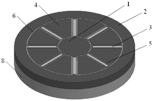
[0053] This embodiment provides a MOS device with an annular channel region, see figure 1 , which includes a substrate 8 and a source 1, a drain 2, a gate 3 and a channel region 4 arranged on the substrate 8, wherein the drain 2 is located at the periphery of the source 1, and the channel region 4 is located at the source 1 and the drain Between the poles 2, the shape of the channel region 4 is ring-shaped, along the direction from the source 1 to the drain 2, a plurality of channels 5 are provided on the surface of the channel region 4, and the side walls and bottoms of the channels 5 are channel functional areas. The gate 3 is located in the channel 5 .

[0054] Compared with the prior art, in the MOS device with an annular channel region provided in this embodiment, the channel region 4 is an annular channel region, and a channel is opened on the surface of the channel region 4 along the direction from the source 1 to the drain 2 5. The channel functional area is the sidew...

Embodiment 2

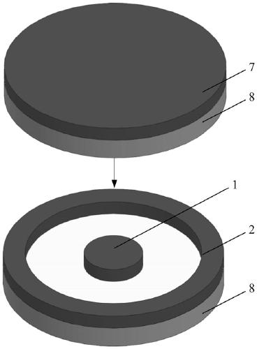
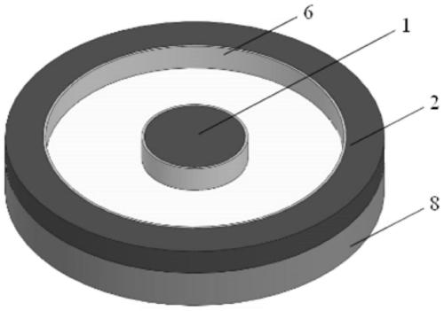
[0063] This embodiment provides a method for preparing a MOS device with an annular channel region, see Figure 2 to Figure 6 , for preparing the MOS device with an annular channel region provided in Example 1, the above preparation method includes the following steps:

[0064] Step 1: providing a substrate 8, forming a source 1 and a drain 2 on the surface of the substrate 8;

[0065] Step 2: epitaxially grow the channel material between the source 1 and the drain 2 to form the channel region 4, by means of chemical mechanical polishing (for example, thermal oxidation, the thermal oxidation temperature is 750°C-850°C, the thermal oxidation time 1min~10min) to smooth the surface, wherein the doping concentration is controlled at 1E16 / cm 3 ~1E18 / cm 3 (for example, 1E17 / cm 3 ~5E17 / cm 3 ), the doping type of the channel region 4 is opposite to that of the source 1 and the drain 2;

[0066] Step 3: Etching and epitaxial channel material (using SiCl 4 , SiH 2 Cl 2 as the ra...


PUM

PropertyMeasurementUnit
thicknessaaaaaaaaaa

Abstract

The invention discloses an MOS device with an annular channel region and a preparation method of the MOS device, belongs to the technical field of MOS devices, and solves the problems of short channeleffect, gate control capability and saturation current reduction of a planar MOS device with a small size (such as nanoscale) in the prior art. The MOS device comprises a source electrode, a drain electrode, a grid electrode and a channel region, the drain electrode is located on the periphery of the source electrode, the channel region is located between the source electrode and the drain electrode, and the channel region is annular; and a plurality of channels are formed in the surface of the channel region in the direction from the source to the drain, and the grid is located in the channels. The preparation method comprises the following steps: forming a source electrode and a drain electrode; forming a channel region between the source electrode and the drain electrode; etching the surface of the channel region along the direction from the source electrode to the drain electrode, and extending a channel material to form a channel; and forming a gate in the channel. According to the MOS device and the preparation method thereof, the area of a current channel can be expanded, and the saturation current is improved.

Description

technical field [0001] The present application relates to a MOS device, in particular to a MOS device with an annular channel region and a preparation method thereof. Background technique [0002] With the continuous miniaturization of semiconductor devices, in order to meet the design requirements for turn-on voltage and saturation current, three-dimensional devices (such as Finfet and nanowires, etc.) are becoming the development direction of the industry. However, because the 3D device process (for example, Fin manufacturing process) is relatively complex and requires high equipment capabilities, in comparison, the planar device process still has considerable cost and process advantages, and will coexist with 3D devices for a considerable period of time. . [0003] In the existing planar device technology, a symmetrical source-drain structure is generally adopted. However, as the channel size continues to decrease, especially after entering the nanometer scale, the short...

Claims


Application Information

Patent Timeline
Patent Type & Authority Applications(China)
IPC IPC(8): H01L29/10H01L29/78H01L21/336
CPCH01L29/1037H01L29/7833H01L29/66492
Inventor 刘金彪王桂磊李俊峰王垚
Owner INST OF MICROELECTRONICS CHINESE ACAD OF SCI
Why Eureka
Try Eureka