Thermal-stacking infrared sensor and mfg. method thereof

An infrared sensor, thermopile technology, applied in instruments, scientific instruments, photometric methods, etc., can solve the problems of unoptimized impurity concentration, reduced S/N ratio, high resistivity, etc., to expand infrared absorption rate or Absorbable wavelength range, excellent S/N ratio, effect of improving S/N ratio

Inactive Publication Date: 2005-05-25
ISHIZUKI ELECTRONICS
View PDF1 Cites 0 Cited by
  • Summary
  • Abstract
  • Description
  • Claims
  • Application Information

AI Technical Summary

Problems solved by technology

However, since the mobility of holes, which are the majority carriers of p-type polysilicon, is low, the resistivity is high
Therefore, there is a disadvantage that the accuracy is not good when used as a sensor of a non-contact thermometer in order to reduce the S / N ratio of the output voltage and Johnson noise.
Therefore, even if it is made as thin as about 10 microns in thickness, the thermal insulation between the hot junction part in the temperature sensing part made of the absorbing film and the cold junction part formed on the substrate is not good, and the temperature sensitivity per unit infrared incident power Partial temperature rises and falls, and as a result, there is a problem that the output voltage drops
[0041] In addition, even if the thermoelectric material uses p-type and n-type polysilicon to increase the apparent chargeability, there will be the following disadvantages: as described above, due to the specific mobility Low, so the resistivity is high. Compared with n-type silicon, the S / N ratio between the output voltage and Johnson noise is low. As in the previous example, when used as a sensor of a non-contact thermometer, the accuracy decreases.
[0042] In addition, since the pattern layout of polysilicon is not laid out on the entire film diaphragm part, cracks are easy to form due to stress concentration during anisotropic etching, so there is a problem of lower yield, or there is a problem that the concentration of impurities is not optimal. Optimizing, the problem that the S / N ratio cannot be achieved as a thermal pile infrared sensor

Method used


Image

  • Thermal-stacking infrared sensor and mfg. method thereof
  • Thermal-stacking infrared sensor and mfg. method thereof
  • Thermal-stacking infrared sensor and mfg. method thereof

Examples


Embodiment 1

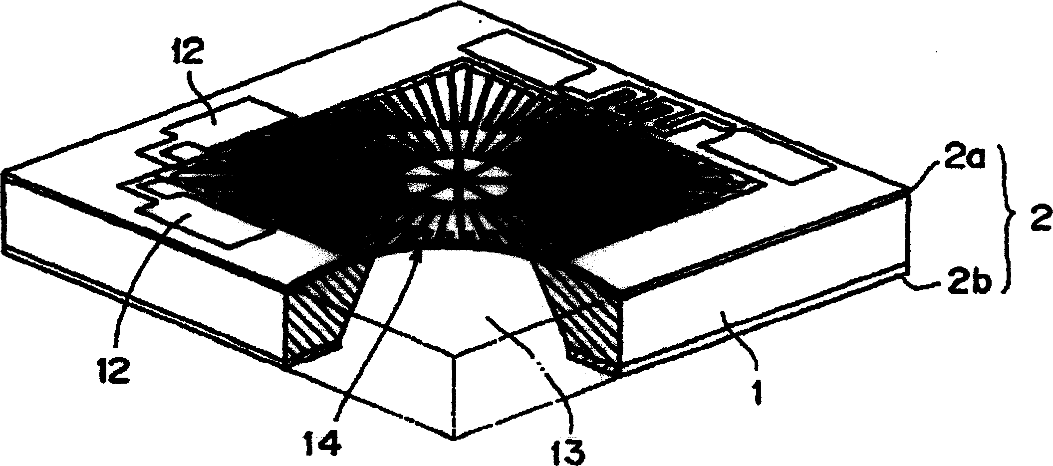
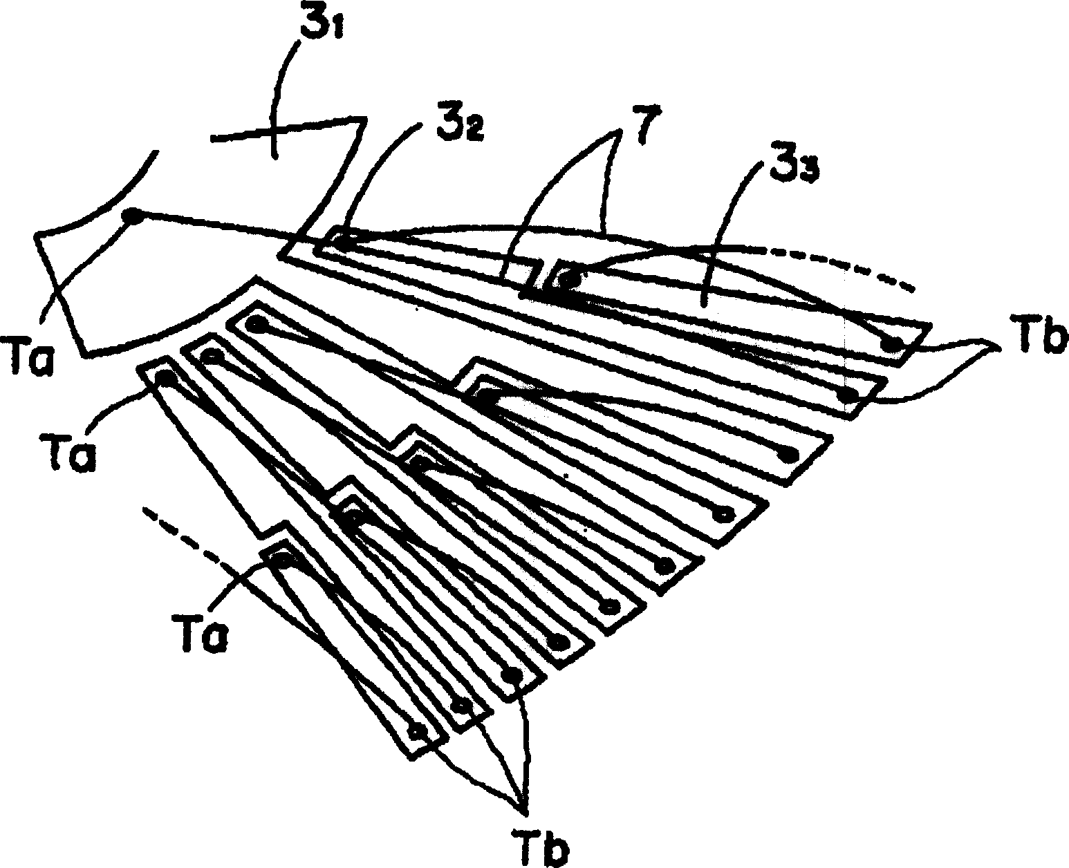
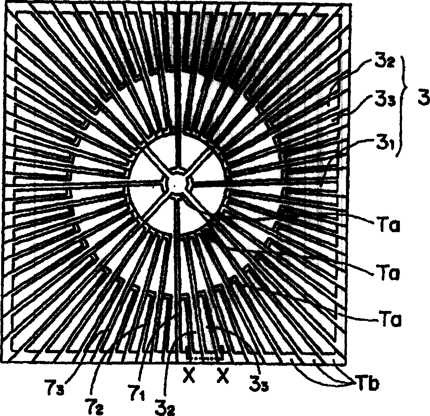
[0180] refer to figure 1 ~ Fig. 6 illustrates Embodiment 1 of the present invention. figure 1 The oblique view of the partial cutout in FIG. 2 shows the thermal pile element (chip) of the thermal pile infrared sensor of the present invention. figure 2 It is an explanatory drawing for explaining the thermal-pile infrared sensor of the present invention. Figure 3(a) is figure 1 The plan view of the polysilicon layer, omits the illustration of the insulating film, passivation film and resin absorbing film, etc., Fig. 3(b) is the X-X sectional view of Fig. 3(a) when the insulating film has been formed. Figure 4 A partial plan view of is showing the outline of the thermal-pile infrared sensor of this embodiment. Figure 5 is the case where the insulating film has been formed Figure 4 Partial floor plans shown in. 6( a ), ( b ) are schematic cross-sectional views of forming a passivation film or an infrared absorption film on a thermopile infrared sensor.

[0181] exist ...

Embodiment 2

[0212] refer to Figure 7 ˜ FIG. 9 illustrates Embodiment 2 of the thermal-pile infrared sensor of the present invention. Figure 7 The schematic diagram shows half of the diagram of a thermopile infrared sensor. Figure 8 It is an enlarged key part schematic showing 1 / 4 of the whole figure. In addition, in Figure 7 , Figure 8 In , the insulating film or passivation layer etc. are omitted. Figure 9(a)~(d) is Figure 8 The film configuration of the A-A, B-B, C-C, and D-D cross-sections shown.

[0213] The purpose of this embodiment is to make the n-type polysilicon layer 3 of embodiment 1 1 ~3 3 The resistance decreases and the S / N ratio is improved, so the film thickness of the n-type polysilicon layer is formed thicker, Figure 7 Its graph is shown. In this embodiment, as in Embodiment 1, a single crystal silicon substrate having a cavity portion is used, and insulating films are formed on both surfaces thereof. As the n-type polysilicon layer of the thermoelectri...

Embodiment 3

[0220] refer to Figure 10 An embodiment of the thermal-pile infrared sensor of the present invention will be described with reference to FIG. 11 . Figure 10 shows the outline of the 1 / 4 figure of this embodiment, and Fig. 11 shows Figure 10 The film composition of A-A, B-B, C-C, D-D, E-E surface. In this example, if Figure 10 , as shown in FIG. 11, adopting the method of disposing the metal thin film layer 7 on the insulating film 2a, it is no longer necessary to cover the patterned n-type polysilicon layer described above with the insulating film 4, and form a polysilicon layer on the insulating film 4. Manufacturing process of the opening portion 15 . Therefore, the manufacturing method of Example 3 is a manufacturing process in which the insulating film 4 forming the opening portion is removed from the manufacturing method of Example 1, and thus detailed description thereof will be omitted.

[0221] exist Figure 10 As in FIG. 11, in this embodiment, on the insulat...


PUM

PropertyMeasurementUnit
electrical resistivityaaaaaaaaaa
thicknessaaaaaaaaaa
thicknessaaaaaaaaaa

Abstract

A thermopile infrared sensor with improved output voltage-Johnson noise S/N ratio, infrared absorption characteristics, and production yield, and a manufacturing method thereof. A thermoelectric element is formed on a substrate with a cavity, and by means of the contact between the polysilicon layer and the metal thin film layer, a hot junction part is formed on the chip center side of the polysilicon layer, and a cold junction part is formed on the peripheral side of the chip, and used The metal thin film layer connects the hot junction part and the adjacent cold junction part to form a column of thermoelectric elements connected in series.

Description

technical field [0001] The present invention relates to a thermal-pile infrared sensor and a manufacturing method thereof, in particular to a thermal-pile infrared sensor that improves the S / N ratio by improving the thermocouple pattern structure of the sensor, and improves the yield rate during its manufacture. A method for manufacturing a heat-pile infrared sensor. Background technique [0002] Generally speaking, the heat balance formula of thermal infrared sensor can be expressed as follows. [0003] [Formula 1] [0004] C·δT / dt+G·δT=W...(1) [0005] Among them, C is the heat capacity, δT is the temperature change of the light receiving part, G is the heat conduction between the light receiving part and the surrounding, and W is the light receiving power. Press W=W at the received light power W 0 When exp(jωt) changes, δT can be expressed as follows. [0006] [Formula 2] [0007] |δT|=W 0 / G(1+τ 2 ω 2 ) 1 / 2 ......(2) [0008] Among them, the thermal time const...

Claims


Application Information

Patent Timeline
Patent Type & Authority Patents(China)
IPC IPC(8): G01J5/12
CPCG01J5/12H01L2224/48091H01L2224/45144H01L2924/00014H01L2924/00
Inventor 远藤治之布施武士松舘直史田中靖崇岡田俊一
Owner ISHIZUKI ELECTRONICS
Why Eureka
Try Eureka