Micron-gap different-surface interdigital photoconductive switch

A photoconductive switch, interdigitated technology, applied in circuits, electrical components, semiconductor devices, etc., can solve the problems of low life, easy breakdown of photoconductive switches, etc., to improve withstand voltage, easy to trigger light energy distribution, The effect of a uniform transient operating electric field

Pending Publication Date: 2020-06-05
XIAN UNIV OF TECH
View PDF11 Cites 3 Cited by
  • Summary
  • Abstract
  • Description
  • Claims
  • Application Information

AI Technical Summary

Problems solved by technology

[0003] The purpose of the present invention is to provide a micron-gap different-plane interdigitated photoconductive switch, which solves the problem that the photoconductive switch is easily broken down under high electric field, which leads to its low life and affects the application under higher electric field.

Method used


Image

  • Micron-gap different-surface interdigital photoconductive switch
  • Micron-gap different-surface interdigital photoconductive switch
  • Micron-gap different-surface interdigital photoconductive switch

Examples


Embodiment Construction

[0022] The present invention will be described in detail below in conjunction with the accompanying drawings and specific embodiments.

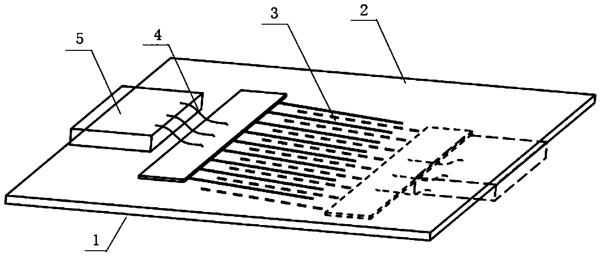
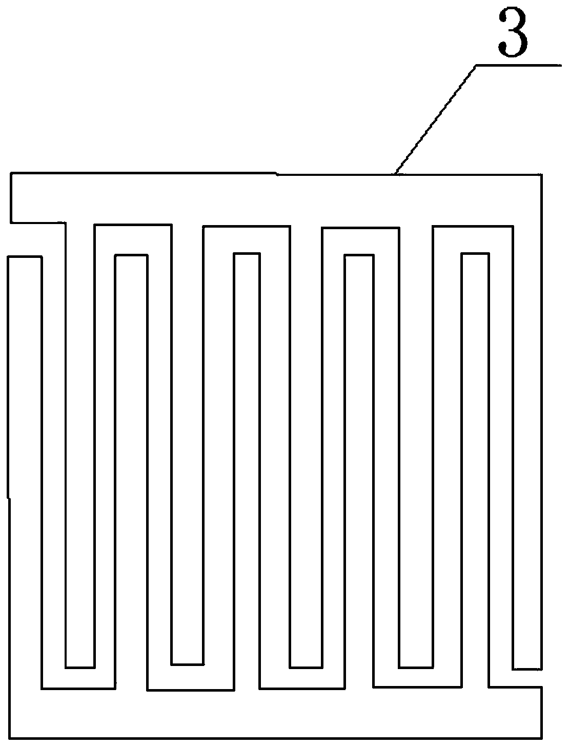
[0023] The present invention adopts a kind of interdigitated interdigitated photoconductive switch with micron gap, such as figure 1 As shown, a substrate 1 is included, and an ion sputtering passivation layer 2 is plated on the substrate 1. The interdigitated electrode 3 is interspersed and connected longitudinally in the substrate 1, and the two plates of the interdigitated electrode 3 are respectively connected to the transmission line 5.

[0024] Both the width and the gap of the interdigital electrodes 3 are 5 μm.

[0025] The side length of the array of interdigitated electrodes 3 is 3 mm.

[0026] The preparation process of the interdigitated electrode 3 is as follows: the substrate is placed in a mixed solution of trichlorethylene, acetone, and methanol in any ratio, cleaned in an ultrasonic bath, and the photoresist is spin-coated. ...


PUM

PropertyMeasurementUnit
widthaaaaaaaaaa
thicknessaaaaaaaaaa
thicknessaaaaaaaaaa

Abstract

The invention discloses a micron-gap different-surface interdigital photoconductive switch which comprises a substrate, an ion sputtering passivation layer is plated on the substrate, an interdigitalelectrode is longitudinally connected in the substrate in an interpenetrating manner, and two polar plates of the interdigital electrode are respectively connected with a transmission line. Accordingto the invention, a small-gap different-surface interdigital electrode is used, so that uniform distribution of light energy is easy to trigger, and the problem of synchronism of trigger light pulsesis solved. A traditional transverse electrode structure is replaced by the different-plane interdigital electrode structure, multi-channel carrier transport is formed in the photoconductive switch through laser cascade triggering, and filamentous current distribution is dispersed, so that a transient working electric field in the photoconductive switch is uniformized, and the voltage endurance capability of the switch is improved.

Description

technical field [0001] The invention belongs to the technical field of electrical engineering equipment, and in particular relates to a different-plane interdigitated photoconductive switch with a micron gap. Background technique [0002] The basic research on the application of semi-insulating GaAs PCSS has entered the research stage of using different combinations to meet the needs of power, repetition frequency, and electrical pulse width under different backgrounds, and is committed to exploring the nonlinear working mode of PCSS induced by weak light under strong electric fields , corresponding to the physical mechanism under certain conditions. However, the small power capacity and low lifetime of GaAs PCSS due to the filamentary current generated in the nonlinear operation mode is still a difficult problem to be solved. For the problem of low switch life caused by GaAs PCSS filamentary current generation, it can be improved by changing the structure and materials use...

Claims


Application Information

Patent Timeline
Patent Type & Authority Applications(China)
IPC IPC(8): H01L31/0224H01L31/0216H01L31/18
CPCH01L31/022408H01L31/02161H01L31/18Y02P70/50
Inventor 徐鸣刘晓斐刘锴董航天王毅
Owner XIAN UNIV OF TECH
Why Eureka
Try Eureka