Organic photodiode, X-ray detector and preparation method thereof

A photodiode and X-ray technology, applied in the field of detection, can solve the problems of slow switching speed of TFT and high manufacturing cost of X-ray detectors, and achieve the effects of improving switching rate, sensitivity and external quantum efficiency.

Pending Publication Date: 2020-06-05
SHANGHAI IRAY TECH
View PDF10 Cites 5 Cited by
  • Summary
  • Abstract
  • Description
  • Claims
  • Application Information

AI Technical Summary

Problems solved by technology

[0006] In view of the shortcomings of the prior art described above, the object of the present invention is to provide an organic photodiode, an X-ray detector and a preparation method thereof, which are used to solve the problem of photodiodes and X-ray detection based on a-Si materials in the prior art. The high cost of device preparation and the slow switching speed of X-ray detector TFT

Method used


Image

  • Organic photodiode, X-ray detector and preparation method thereof
  • Organic photodiode, X-ray detector and preparation method thereof
  • Organic photodiode, X-ray detector and preparation method thereof

Examples


Embodiment 1

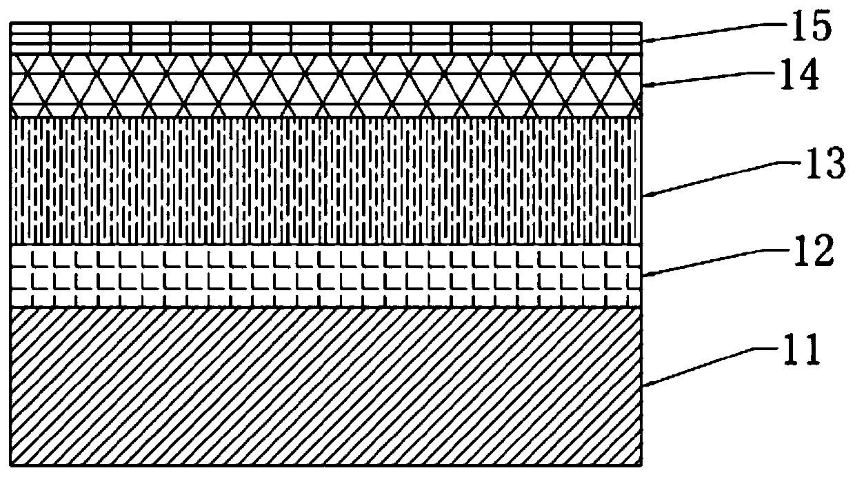
[0047] refer to figure 1 , the present embodiment provides an organic photodiode, which includes a first conductive transport layer 12, a P3HT:PCBM active layer 13, a second conductive transport layer 14, and a transparent top electrode layer stacked in sequence from bottom to top 15.

[0048] The organic photodiode of this embodiment can be produced with low-cost equipment, thereby simplifying the preparation process and saving costs; in the organic photodiode, the bandgap of the P3HT:PCBM active layer 13 is adjustable, Therefore, the external quantum efficiency of the organic photodiode can be improved, thereby improving the sensitivity of the X-ray detector.

[0049] As an example, the first conductive transport layer 12 includes an electron transport layer, and the second conductive transport layer 14 includes a hole transport layer; or the first conductive transport layer 12 includes a hole transport layer, and the second conductive transport layer 14 includes a hole tra...

Embodiment 2

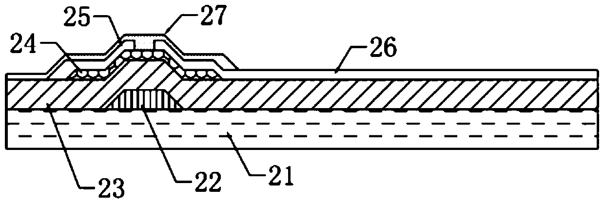
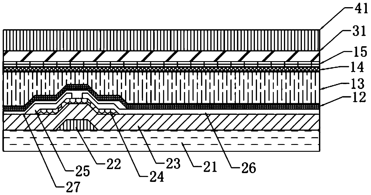
[0072] refer to Figure 4 This embodiment provides an X-ray detector, which differs from Embodiment 1 mainly in that the thin-film transistor of the X-ray detector adopts a top-gate organic thin-film transistor, so as to expand the application range of the X-ray detector.

[0073] Specifically, the X-ray detector includes a top gate organic thin film transistor, an organic photodiode located on the top gate organic thin film transistor, a passivation layer 31' and a scintillator layer 41'. Wherein, the top gate organic thin film transistor includes a substrate 21', a source metal electrode 25', a drain metal electrode 26', a channel layer 24', a gate insulating layer 23', a gate metal electrode 22' and passivation protective layer 27'; the organic photodiode includes a first conductive transport layer 12', a P3HT:PCBM active layer 13', a second conductive transport layer 14' and a transparent top electrode layer 15'. Wherein, the structure, material and manufacturing method o...


PUM

PropertyMeasurementUnit
thicknessaaaaaaaaaa
thicknessaaaaaaaaaa
thicknessaaaaaaaaaa

Abstract

The invention provides an organic photodiode, an X-ray detector and a preparation method of the X-ray detector. The organic photodiode and an organic thin film transistor are prepared by adopting a solution method, so that low-cost equipment can be adopted for production, the preparation process is simplified, and the cost is saved. The organic photodiode and the organic thin film transistor are combined, which is suitable for preparing the flexible X-ray detector. In the organic photodiode, the band gap of an organic active layer is adjustable, so that the external quantum efficiency of the organic photodiode can be improved, and the sensitivity of the X-ray detector is further improved. In the organic thin film transistor, the carrier mobility of an organic channel layer is relatively high, so that the switching rate of the organic thin film transistor can be improved.

Description

technical field [0001] The invention belongs to the technical field of detection, and relates to an organic photodiode, an X-ray detector and a preparation method thereof. Background technique [0002] Direct Digital Radiography (DR) appeared in the 1990s because of its excellent image quality, excellent post-processing function, low X-ray dose, efficient storage, efficient transmission, resource saving and work efficiency With a series of remarkable advantages, it has been more and more widely used in medical imaging, industrial testing and other fields. [0003] The detector is the most critical component in the DR system. It is composed of a photoreceptor array (Sensor array) and peripheral circuit modules. It can convert the X-ray signal after passing through the object into an electrical signal, and finally the image is processed by the computer. In the mainstream indirect detectors, X photons are first converted into low-energy photons by scintillators, and then captu...

Claims


Application Information

Patent Timeline
Patent Type & Authority Applications(China)
IPC IPC(8): H01L51/42H01L51/46H01L51/48H01L27/30G01T1/20
CPCG01T1/2018H10K39/36H10K71/12H10K85/215H10K30/00Y02E10/549
Inventor 韦小庆金利波
Owner SHANGHAI IRAY TECH
Why Eureka
Try Eureka