Multi-surface treatment process for PCB

A PCB board and surface treatment technology, which is applied in the field of processing technology combining multiple surface treatments of PCB boards, can solve the problems that immersion silver does not have the physical strength of chemical nickel plating/immersion gold, loses luster, and surface treatment processes are difficult to achieve. , to achieve the effect of fast and efficient production process, strong tolerance and low production cost

Pending Publication Date: 2020-06-12
惠州市纬德电路有限公司
View PDF4 Cites 4 Cited by
  • Summary
  • Abstract
  • Description
  • Claims
  • Application Information

AI Technical Summary

Problems solved by technology

[0008] 6. Immersion silver: The complexity of the immersion silver process is between organic coating and chemical nickel plating/immersion gold, and the process is relatively simple and fast; even if exposed to heat, humidity and polluted environments, silver can still maintain good Solderability, but will lose luster; immersion silver does not have the good physical strength of electroless nickel/immersion gold;
[0011] In the p

Method used


Image

  • Multi-surface treatment process for PCB

Examples


Embodiment 1

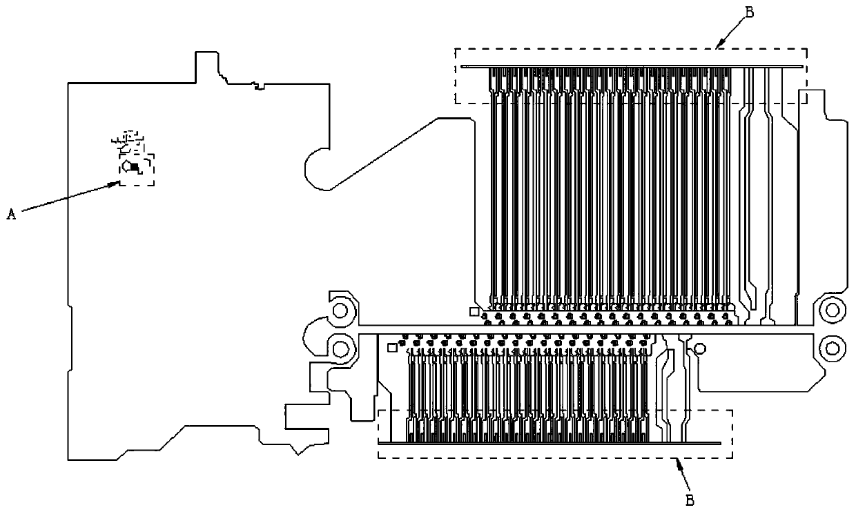
[0028] Such as figure 1 Shown is the PCB board to be surface treated in this embodiment, wherein the A area is the BGA area, which needs to be organically coated; the B area is the gold finger area, which needs to be electroplated with hard gold; the remaining areas need to be subjected to immersion gold treatment; The surface treatment process includes the following steps:

[0029] Step 1: Install a barrier film on the surface of the PCB board, the barrier film covers the non-copper-plated area on the surface of the PCB board, the barrier film is provided with a window, and the window covers the A area of ​​the PCB board (ie, the BGA area) and is made into a printing screen;

[0030] Step 2: Use the screen plate made of the above-mentioned film to coat the BGA area of ​​the PCB board with selective ink that resists immersion gold potion, and then perform drying treatment;

[0031] Step 3: Carry out immersion gold treatment on the PCB board;

[0032] Step 4: Cover the PCB bo...


PUM


Abstract

The invention discloses a multi-surface treatment process for a PCB. The multi-surface treatment process comprises the following steps: 1, arranging a barrier film on the surface of the PCB; 2, coating the BGA area of the PCB with selective ink resistant to nickel-gold deposition liquid medicine; 3, carrying out nickel-gold deposition treatment on the PCB; 4, covering the PCB with a blue protective film; 5, carrying out hard gold electroplating treatment on the PCB; 6, removing the blue protective film and the selective ink on the surface of the PCB; and 7, carrying out OSP surface coating onthe PCB. According to the various surface treatment processes of the PCB, the selective ink is matched with the blue protective film; the three surface treatment processes of nickel-gold deposition, hard gold electroplating and organic coating are orderly applied to the same PCB, so that the BGA area in the PCB is good in surface mounting performance, the golden finger or key area is resistant toabrasion and plugging, and the whole PCB is high in tolerance to the environment and meets the lead-free assembly requirement.

Description

technical field [0001] The invention relates to the field of PCB board processing, in particular to a processing technology combining multiple surface treatments of the PCB board. Background technique [0002] After the PCB board is processed, the copper plating on the surface of the outer layer board will gradually oxidize without surface treatment, which will affect the solderability and electrical properties of the PCB board. Therefore, the PCB board needs to be surface treated after processing. The common surface The treatment process includes: [0003] 1. Hot air leveling: hot air leveling is also known as hot air solder leveling (commonly known as HASL, which is divided into two types: lead HASL and lead-free HASL); it has the advantages of simple process and good solderability, but the flatness is relatively poor. Not conducive to surface mount; [0004] 2. Coating organic solderability preservative (OSP): OSP is the abbreviation of Organic Solderability Preservativ...

Claims


Application Information

Patent Timeline
IPC IPC(8): H05K3/22H05K3/28
CPCH05K3/22H05K3/28
Inventor 李建根
Owner 惠州市纬德电路有限公司
Why Eureka
Try Eureka