
Mini lamp bead, manufacturing method, backlight source and display equipment

A technology of backlight source and lamp beads, applied in the field of production method, backlight source and display equipment, and mini lamp beads, can solve the problems of increased power, more heat generation, and small luminous angle of MINILED, and achieves reduction of power and heat generation. , the effect of reducing the number of

Pending Publication Date: 2020-06-19
SHENZHEN SKYWORTH RGB ELECTRONICS CO LTD
View PDF0 Cites 7 Cited by
  • Summary
  • Abstract
  • Description
  • Claims
  • Application Information

AI Technical Summary

Problems solved by technology

[0003] However, the existing MINI LEDs have a small luminous angle and basically emit light from the front. There is basically no light emitted from the side of the lamp beads, so that the energy between the lamp beads is less; furthermore, dark areas are generated between the lamp beads.
In order to achieve a good imaging effect, it is necessary to densely arrange the MINI LED lamp beads on the backlight, and the distance between the lamp beads is about 3mm, which increases the cost of the backlight source, and increases the power and heat production during use. many

Method used


Image

  • Mini lamp bead, manufacturing method, backlight source and display equipment
  • Mini lamp bead, manufacturing method, backlight source and display equipment
  • Mini lamp bead, manufacturing method, backlight source and display equipment

Examples


Embodiment 1

[0050] In order to solve the above technical problems, the present invention provides a mini lamp bead, which can realize side light emission and increase the brightness between lamp beads, thereby expanding the distance between lamp beads and reducing the density of lamp beads on the backlight, thereby reducing cost and power consumption. As an illustration, in the embodiment, the MINI LED lamp bead that appears in the following refers to the miniature lamp bead mentioned above.

[0051] like Figure 4 As shown, the MINI LED light bead includes a light source 20 and a microlens 24; the microlens 24 surrounds the light source 20; The surface is flush. like Figure 4 The direction shown in is a reference to define up, down, left, right, etc. orientations, which are only used to describe the relative positions of each component, and should not be used as limitations on this application.

[0052] Described microlens 24 is provided with a cavity, and described light emitting so...

Embodiment 2

[0081] like Figure 7 As shown, this embodiment provides a backlight source, including a substrate 30 on which the miniature lamp beads (MINI LED lamp beads) are arranged in an array; the substrate 30 is a circuit board.

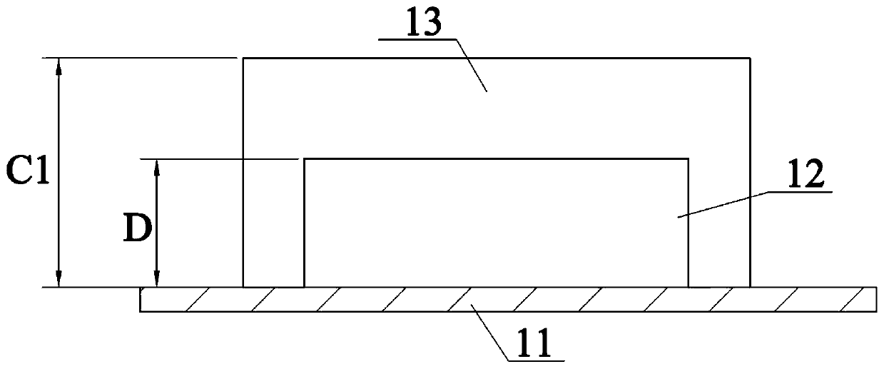
[0082] The MINI LED lamp beads can realize a large-angle light emitting range of ±70°, increasing the light energy between the MINI LED lamp beads. At the same time, the height C2 of the MINI LED lamp beads is about 0.65mm, so that the MINI LED lamp beads have a larger optical distance, thereby increasing the light mixing effect among the MINI LED lamp beads. Therefore, the distance A3 between the MINI LED lamp beads on the backlight of the present application can be about 10mm, and then the density of the MINI LED lamp beads on the substrate 30 can be reduced, and the number of MINI LED lamp beads in the backlight source of the present application per unit area can be reduced. Compared with the traditional backlight, the number of MINI LED lamp beads can b...

Embodiment 3

[0085] This embodiment provides a display device, including a display panel, an optical component, and the backlight source. The optical component is disposed between the display panel and the backlight source. The light generated by the backlight source is irradiated on the display panel after passing through the optical assembly, so as to form an image on the display panel.

[0086] In the display device of the present application, the density of MINI LED lamp beads on the backlight source is small; in use, energy consumption and heat generation can be reduced, thereby ensuring the normal operation of the backlight source, thereby ensuring that the display device can image normally.


PUM


Abstract

The invention discloses a mini lamp bead, a manufacturing method, a backlight source and display equipment, and relates to the technical field of display. The mini lamp bead comprises a light-emittingsource and a micro lens covering the light-emitting source. The micro lens is provided with a first light-emitting surface for realizing upward transmission of light and a second light-emitting surface for realizing lateral transmission of light. The backlight source comprises a substrate, and mini lamp beads are arranged on the substrate in an array mode. The display equipment comprises the backlight source. The manufacturing method comprises the steps of manufacturing a crystal ingot; cutting the crystal ingot into a wafer; generating an epitaxial layer on the wafer; manufacturing an electrode on the epitaxial layer to form an LED chip; and a base and a micro lens are additionally arranged on the LED chip. Lateral light emitting of the mini lamp beads can be achieved, the density of themini lamp beads on the backlight source is reduced, and then cost and power consumption are reduced.

Description

technical field [0001] The invention relates to the field of display technology, in particular to a mini lamp bead, a manufacturing method, a backlight source and a display device. Background technique [0002] As display devices such as mobile phones, iPads, and smart TVs are developing in the direction of lightness, thinness, and better image quality. Among them, as a new generation of display technology, mini lamp beads are popular in the market due to their small size, thin thickness, high brightness, millimeter-level pixel division, high-precision dynamic backlight effects, etc., such as MINI LED, mini OLED and other mini LED lighting Lamp beads. [0003] However, the existing MINI LEDs have a small luminous angle and basically emit light from the front. There is basically no light emitted from the side of the lamp beads, so that the energy between the lamp beads is less; furthermore, dark areas are generated between the lamp beads. In order to achieve a good imaging ...

Claims


Application Information

Patent Timeline
IPC IPC(8): G09F9/00H01L33/58H01L33/52H01L33/00
CPCG09F9/00H01L33/58H01L33/52H01L33/005
Inventor 胡珊珊
Owner SHENZHEN SKYWORTH RGB ELECTRONICS CO LTD
Learn More