Compensation method and device for bit line leakage current of static random access memory
A static random and compensation method technology, applied in static memory, digital memory information, information storage and other directions, can solve the problems of affecting the readout rate, increase the area of SRAM cells, etc., to improve the circuit working speed, reduce the reading working time, improve the The effect of discharge rate
- Summary
- Abstract
- Description
- Claims
- Application Information
AI Technical Summary
Problems solved by technology
Method used
Image
Examples
Embodiment 1
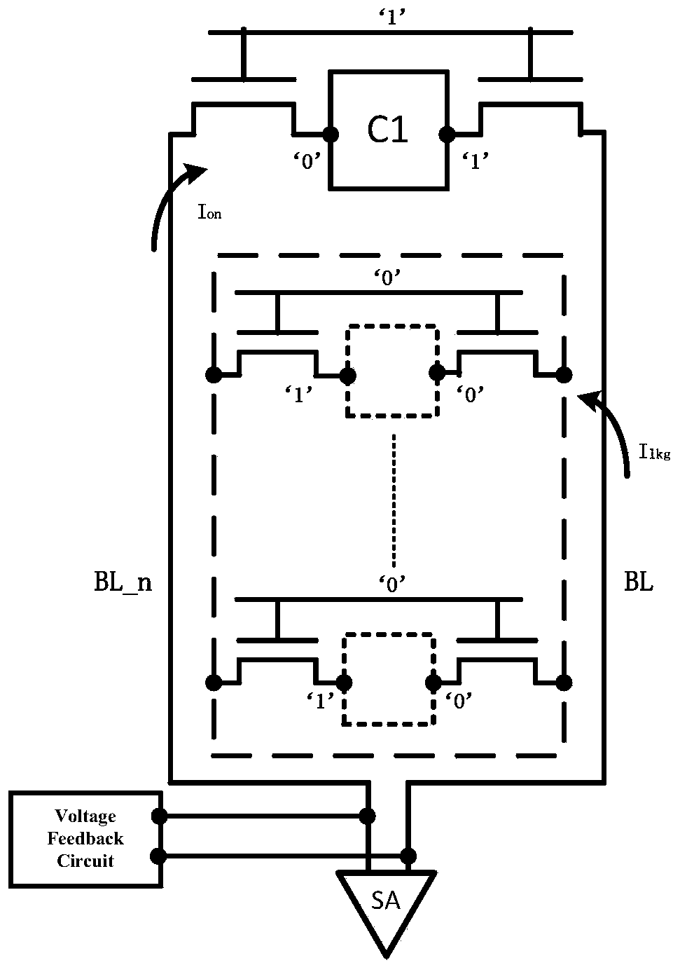
[0033] like figure 2 As shown, when reading the C1 cell, the bit line is precharged to a high potential, and a leakage current will be formed between the bit line and the "0" node inside the SRAM cell, and the leakage current will affect the discharge current on the bit line. As the scale of the circuit increases, more and more SRAM cells are connected to the bit line, and the cells that generate leakage current will also increase. When the total leakage current is large enough that the discharge current on the bit line BL is close to or even greater than When the discharge current on BL_n, it will cause read failure. Assuming that each bit line of the SRAM circuit is connected with N SRAM cells, where n cells on BL will generate leakage current, then N-n cells on BL_n will generate leakage current. The leakage current generated by each cell is I lkg , the turn-on current is I on . While reading the SRAM cell C 1 During the process, the total discharge current on the bit...
Embodiment 2
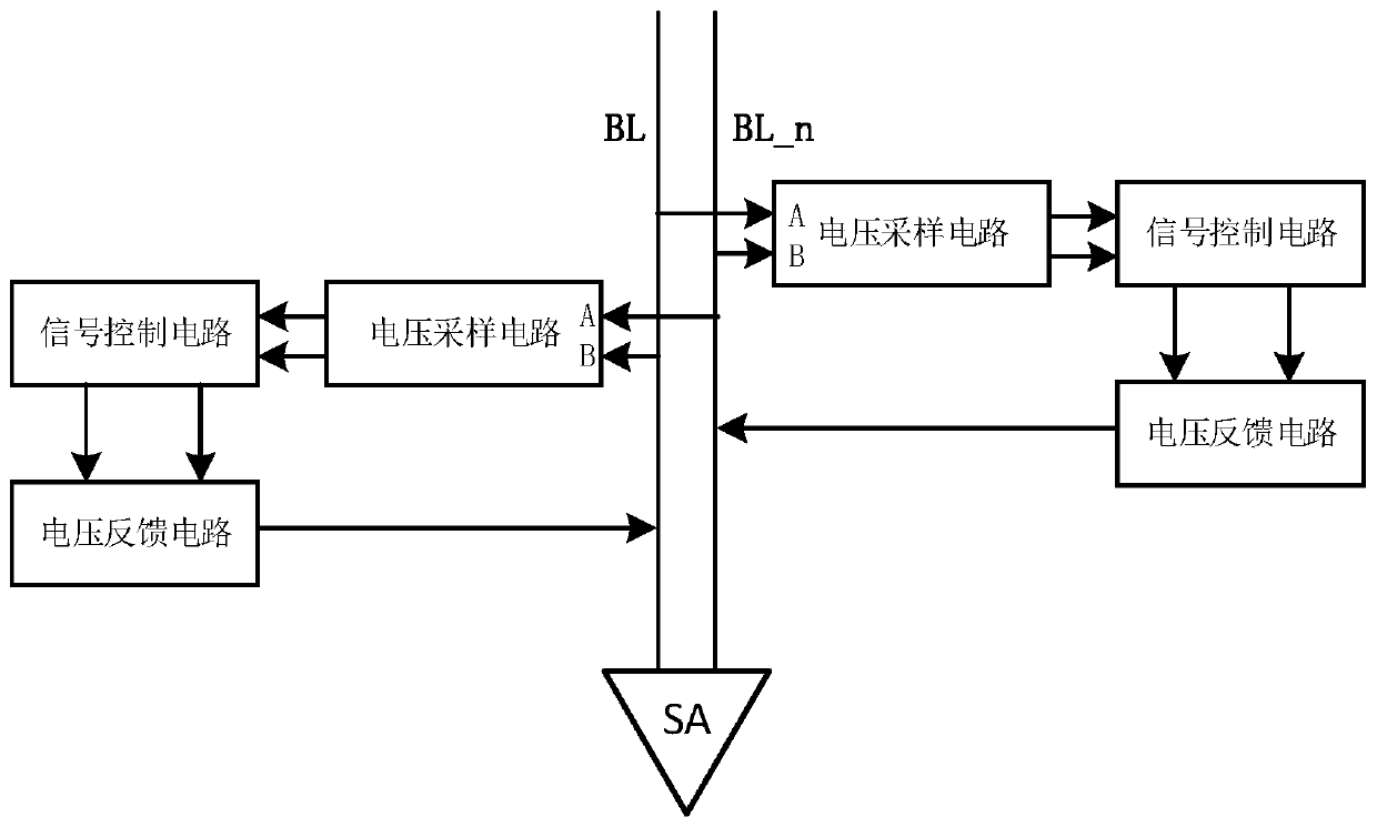
[0047] This embodiment provides a compensation device for bit line leakage current of SRAM, including: at least one compensation module; the compensation module includes:
[0048] A voltage sampling circuit, which collects the discharge currents of two adjacent bit lines; optionally, the voltage sampling circuit is used to sample the voltages of two adjacent bit lines and calculate the rate of voltage change with time, so as to obtain the The discharge current of two adjacent bit lines is described.
[0049] A signal control circuit, configured to receive information collected by the voltage sampling circuit and send a control signal;
[0050] The voltage feedback circuit is used to control the decrease of the voltage of the bit line with a larger discharge current among the two adjacent bit lines, and / or control the increase of the voltage of the bit line with a smaller discharge current among the two adjacent bit lines.
[0051] For this embodiment, there are three optional...
PUM
 Abstract
Description
Claims
Application Information

