A fan-out package and manufacturing method thereof

A manufacturing method and packaging technology, applied in semiconductor/solid-state device manufacturing, electrical components, semiconductor devices, etc., can solve problems such as high parasitic capacitance and inductance, deformation and fracture of passivation layer, signal short circuit, etc., to improve quality and protection ability The effect of improving and increasing firmness

Active Publication Date: 2021-11-09
JOULWATT TECH INC LTD
View PDF4 Cites 0 Cited by
  • Summary
  • Abstract
  • Description
  • Claims
  • Application Information

AI Technical Summary

Problems solved by technology

[0006] However, in the above-mentioned fan-out packaging structure, when there are many input and output ports (I / O) and there is a design where different signal metal layers overlap directly above the chip, the following problems will be brought about: 1. Higher parasitic capacitance and inductance will be introduced ; 2. Crosstalk between different signal layers; 3. The passivation layer is prone to deformation and fracture due to external force, causing the risk of signal short circuit or open circuit

Method used


Image

  • A fan-out package and manufacturing method thereof
  • A fan-out package and manufacturing method thereof
  • A fan-out package and manufacturing method thereof

Examples


Embodiment approach 1

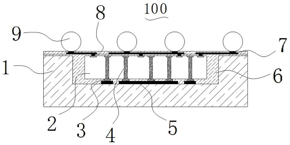
[0045] See figure 2 , figure 2 It is a schematic diagram of the fan-out package structure in a first embodiment of the present invention. As shown, the fan-out package 100 comprising a substrate 1, chip 2, plastic material 6, a first redistribution layer 7, a second redistribution layer 5, and a plurality of solder balls 9. The substrate 1 is typically a semiconductor material, such as silicon, germanium, selenium, or compound semiconductors, organic semiconductors, with a receiving slot on the substrate, and acting as a support is placed the chip, and to assume a portion of the electrical properties.

[0046] Chip 2 is placed on the receiving groove substrate 1, the chip 2 includes a first surface and a second surface opposite the first surface, the first surface 8 is provided with a plurality of input and output ports, the second surface is provided with a plurality of bumps 3, the bumps 3 of the plurality of positions corresponding to a plurality of input and output ports of at...

no. 2 approach

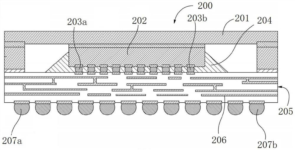
[0064] See Figure 4 , Figure 4 It is a schematic structural diagram of a fan-out package in a second embodiment of the present invention. As shown, in this embodiment, the fan-out package 110 introduces two chips 2a and 2b, each having at least one TSV4 '. The two chips can be a chip of different functions, or the same functional chip, and there is a signal transmission between each other, that is, at least one input / output port of the chip 2a needs to be connected to at least one input and output port of the chip 2b. According to the spirit of the invention, these input and output ports that require interconnect or derive will guide the second surface corresponding to the second surface by TSV4 '.

[0065] In this embodiment, the graphic of the first redistribution layer 7 'and the second redistribution layer 5' needs to guide the first surface to the input and output port 8 'of electrical interconnection or electrical extraction in accordance with the specific circuitry. Exter...

Embodiment approach 2

[0066] The second embodiment gives the package structure of two chips, which should be noted that for two or more multi-chip packages, the invention can also be designed according to the invention of the invention, without the need for creative labor. For the production method of the second embodiment, as the embodiment is substantially the same, only the graphic of the first redistribution layer and the second redistribution layer is designed, the design is required to be designed according to the specific circuitry. The same is the same as the implementation, and will not be described again.

[0067] In summary, the present invention proposes a new fan-out package and a method of fabricating the same, which leads some input and output port ports to the back side by introducing TSV structures in the chip, and then in front of both sides The rearrangement layer structure is designed to reduce the number of redistributed layer metal layers on a single side, thereby reducing the occ...


PUM


Abstract

The present invention is a fan-out package, comprising a substrate, on which an accommodating groove is arranged; at least one chip, located in the accommodating groove of the substrate; and a plastic sealing material, encapsulating and fixing the at least one chip In the accommodating groove of the substrate; wherein, the TSV structure is introduced into the chip, and part of the input and output ports are electrically guided to the back, and then the redistribution layer structure is designed on both the front and back sides, reducing the redistribution layer on one side The number of metal layers reduces the occurrence of parasitic capacitance and signal crosstalk, which improves the stability and reliability of the device.

Description

Technical field [0001] The present invention relates to semiconductor technology, and in particular, package and relates to a method of manufacturing a fan-out. Background technique [0002] Field of semiconductor packaging, packaging requirements with a high degree of integration to TSV (Through Silicon Via, TSV) as the core of 3D IC packaging technology is an important field of high-density packaging. [0003] Meanwhile, as chips become smaller and smaller, I / O number more and more fan-type wafer level package interconnection not meet the requirements. Fanout (fanout) packaging technology as a solution to this conflict solution by reconstituting chip wafer arrangement, the small chip I / O leads outside the body, which is formed larger than the package. [0004] First core fanout one embodiment the chip side up process, when a large positive chip I / O, inevitably varying signals directly above the metal layer overlapping the chip design, the use of polyimide PI therebetween ...

Claims


Application Information

Patent Timeline
Patent Type & Authority Patents(China)
IPC IPC(8): H01L23/48H01L23/488H01L23/31H01L21/50H01L21/56
CPCH01L21/50H01L21/56H01L23/3114H01L23/481H01L23/488H01L24/02H01L2224/02331H01L2224/02372H01L2224/02373H01L2224/02375H01L2224/02379H01L2224/02381H01L2224/16225H01L2224/18H01L2224/32225H01L2224/73204H01L2224/73253H01L2924/15153H01L2924/15311H01L2924/16195H01L2924/00
Inventor 孟繁均陆阳
Owner JOULWATT TECH INC LTD
Why Eureka
Try Eureka