MOS device and manufacturing method

A technology of MOS devices and manufacturing methods, applied in semiconductor/solid-state device manufacturing, semiconductor devices, electrical components, etc., can solve problems such as large parasitic capacitance, and achieve the effects of reducing parasitic capacitance, reducing costs, and reducing short-channel effects

Active Publication Date: 2015-12-09
SHANGHAI HUAHONG GRACE SEMICON MFG CORP
View PDF4 Cites 0 Cited by
  • Summary
  • Abstract
  • Description
  • Claims
  • Application Information

AI Technical Summary

Problems solved by technology

The disadvantages of the existing MOS devices are: since the source-drain region 105a is in contact with the metal contact 107, the area of ​​the source-drain region 105a must be large enough to contain the area of ​​the contact hole of the metal contact 107, In this way, the area of ​​the source-drain region 105a will be larger, and the parasitic capacitance generated between the source-drain region 105a and the substrate will also be larger.

Method used


Image

  • MOS device and manufacturing method
  • MOS device and manufacturing method
  • MOS device and manufacturing method

Examples


Embodiment Construction

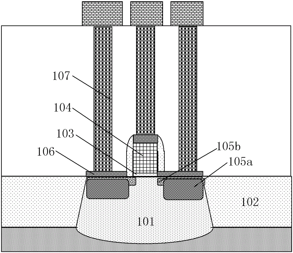
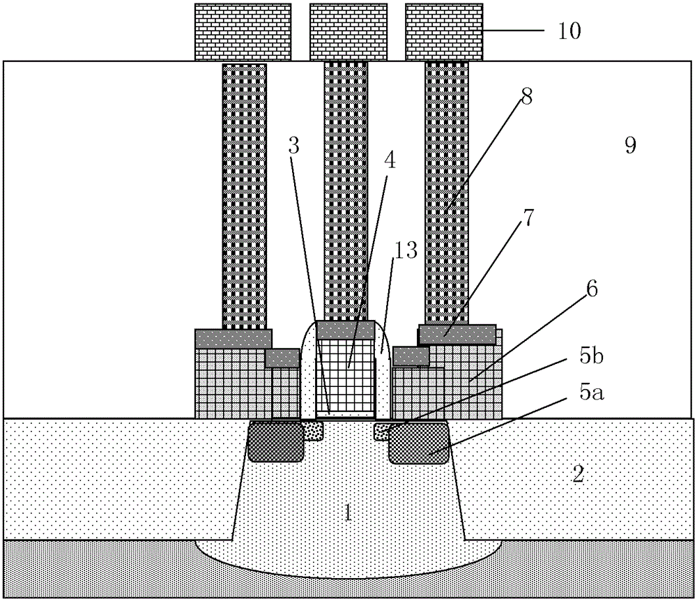
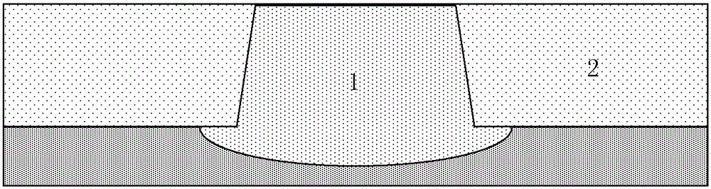
[0038] Such as figure 2 Shown is a schematic structural diagram of a MOS device according to an embodiment of the present invention. The MOS device in the embodiment of the present invention is formed on a silicon substrate, the active region is isolated by the shallow trench field oxygen 2 , and a well region 1 of the second conductivity type is formed in the entire active region.

[0039] The gate is composed of a gate silicon oxide layer 3 and a gate polysilicon layer 4 sequentially formed on the active region, and a side wall 13 is formed on the side wall of the gate. The thickness of the gate silicon oxide layer 3 is 20-100 angstroms; the thickness of the gate polysilicon layer 4 is 1500-2000 angstroms. The composition of the side wall 13 is an oxide film, or a composite film of a nitride film and an oxide film. The well region 1 covered by the gate is a channel region.

[0040] The source and drain regions are formed on both sides of the gate and include a source and...


PUM

PropertyMeasurementUnit
thicknessaaaaaaaaaa
thicknessaaaaaaaaaa
thicknessaaaaaaaaaa

Abstract

The invention discloses a metal oxide semiconductor (MOS) device, and further discloses a manufacturing method of the MOS device. A source-drain region comprises a source-drain mixing region located in an active region and a source-drain polycrystalline silicon layer located on the upper portion of the source region. A source electrode and a drain electrode are led out by forming metal contact on a germanium silicon polycrystalline silicon layer outside the drain polycrystalline silicon layer. Because the area of the source and drain mixing region in the active region does not necessarily contain the area of metal contact, the area of the active region can be made minimum, and performance and integration levels of the device can be improved. The MOS device can reduce stray capacitance between the source-drain region and a substrate, and can be suitable for being applied to the field of radio frequency (RF). The junction depth of the source-drain mixing region is shallow and can reduce short-channel effect and relieve serious length of diffusion (LOD) effect. The manufacturing method of the MOS device can adequately solve the problems of difficulties in an etching stop aspect in the process and isolation optimization between the grid electrode and the source electrode and the drain electrode, and reduce the number of metal layers and cost of the whole bipolar complementary metal-oxide semiconductor (BICMOS) technology.

Description

technical field [0001] The invention relates to the field of semiconductor integrated circuit manufacturing, in particular to a MOS device. The invention also relates to a manufacturing method of the MOS device. Background technique [0002] Semiconductor products have a broad application market. In the fields of industry, agriculture, military and civilian use, semiconductor products play an increasingly important role in control, monitoring, and entertainment. Therefore, a large-scale industry has formed all over the world. Developed countries such as Europe, America and Japan are the first to master the advanced technology from semiconductor design to manufacturing; Asian regions such as South Korea and Taiwan also have a place in semiconductor manufacturing; Having a huge market has also strongly supported the research and development of semiconductor integrated circuit production technology in the last ten years. There are a wide variety of IC products, such as power ...

Claims


Application Information

Patent Timeline
Patent Type & Authority Patents(China)
IPC IPC(8): H01L29/78H01L29/08H01L29/10H01L21/336
Inventor 邱慈云朱东园范永洁钱文生徐向明肖胜安陈帆刘鹏陈雄斌潘嘉刘冬华孙娟袁媛吴智勇黄志刚王雷郭晓波孟鸿林苏波季伟程晓华钱志刚陈福成刘继全孙勤金锋刘梅
Owner SHANGHAI HUAHONG GRACE SEMICON MFG CORP
Why Eureka
Try Eureka