

Fan-out type packaging piece and manufacturing method thereof
A manufacturing method and packaging technology, which are used in semiconductor/solid-state device manufacturing, electrical components, and electrical solid-state devices, etc., can solve problems such as deformation and fracture of passivation layers, high parasitic capacitance and inductance, and short-circuit signals, and achieve improved protection capabilities. The effect of reducing the generation of parasitic capacitance and reducing the number of metal layers
- Summary
- Abstract
- Description
- Claims
- Application Information
AI Technical Summary
Problems solved by technology
Method used
Image

Examples
Embodiment approach 1
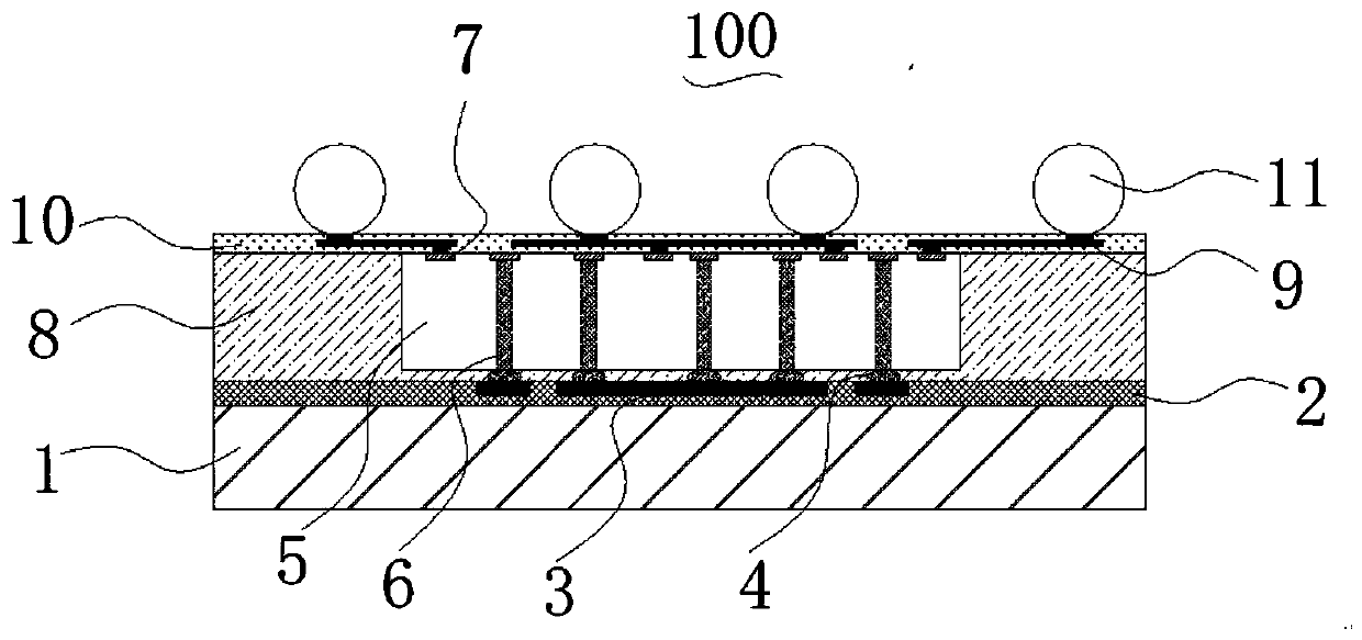
[0046] See figure 2 , figure 2 is a schematic structural view of the fan-out package in the first embodiment of the present invention. As shown in the figure, the fan-out package 100 includes a substrate 1 , a chip 5 , a molding material 8 , a first redistribution layer 9 , a second redistribution layer 3 , and a plurality of solder balls 11 . The substrate 1 acts as a support for the entire device, and at the same time bears a part of the electrical performance. The substrate 1 is usually a semiconductor material, such as silicon, germanium, selenium, or a compound semiconductor, an organic semiconductor, and the like.
[0047]Chip 5 is fixed on the substrate 1 by bonding layer 2, and this bonding layer 2 preferably uses non-conductive bonding material, such as glass glue, epoxy resin or other non-conductive colloids, as shown in the figure, this bonding layer 2 In addition to bonding the chip 5 and the substrate 1 to one of them, the second redistribution layer 2 is also...
no. 2 approach
[0063] See Figure 4 , Figure 4 is a schematic structural diagram of a fan-out package in the second embodiment of the present invention. As shown, in this embodiment, a fan-out package 110 incorporates two chips 5a and 5b, each chip having at least one TSV 6'. These two chips can be chips with different functions, or chips with the same function, and there needs to be signal transmission between each other, that is, at least one input and output port 7' of the chip 5a needs to be connected to at least one input and output port of the chip 5b superior. According to the gist of the present invention, these input and output ports that need to be interconnected or extracted will be electrically guided to the corresponding bump 4' on the second surface through the TSV 6'.
[0064] In this embodiment, the patterns of the first redistribution layer 9' and the second redistribution layer 3' need to guide the input and output ports 7' on the first surface that need to be electrica...
Embodiment approach 2
[0065] Embodiment 2 provides a package structure of two chips. It should be noted that, for more than two multi-chip packages, it can also be designed according to the gist of the invention without creative labor. The manufacturing method of the second embodiment is basically the same as that of the first embodiment, only when designing the patterns of the first redistribution layer and the second redistribution layer, it needs to be designed according to specific circuit requirements. The points that are the same as those in Embodiment 1 will not be repeated here.
[0066] To sum up, the present invention proposes a new fan-out package and its manufacturing method. The package introduces a TSV structure into the chip to electrically guide part of the input and output ports to the back, and then connects the front and back sides of the package. The redistribution layer structure is designed to reduce the number of redistribution layer metal layers on a single side, thereby red...
PUM
 Abstract
Description
Claims
Application Information