A graphene/palladium diselenide/silicon heterojunction self-driven photodetector

A photodetector and silicon heterojunction technology, applied in the field of photodetection, can solve the problems of narrow detection bandwidth, slow response time, difficult integration, etc., and achieve the effect of reducing interface recombination, facilitating separation, and high responsivity

Active Publication Date: 2022-04-01
UNIV OF ELECTRONICS SCI & TECH OF CHINA
View PDF0 Cites 0 Cited by
  • Summary
  • Abstract
  • Description
  • Claims
  • Application Information

AI Technical Summary

Problems solved by technology

[0002] Photodetectors are devices that convert optical signals into electrical signals. Although photodetectors made of traditional three-dimensional materials have good performance and mature manufacturing processes, they also have their shortcomings, such as infrared detectors. HgCdTe needs to work normally in a specific low temperature environment; photoresistors made of cadmium sulfide have a slow response time; silicon photodetectors have a relatively narrow detection bandwidth due to the limitation of silicon itself
Most importantly, detectors made of traditional three-dimensional materials are relatively difficult to integrate due to the severe surface states of three-dimensional materials.

Method used


Image

  • A graphene/palladium diselenide/silicon heterojunction self-driven photodetector
  • A graphene/palladium diselenide/silicon heterojunction self-driven photodetector
  • A graphene/palladium diselenide/silicon heterojunction self-driven photodetector

Examples


Embodiment Construction

[0023] In order to facilitate those skilled in the art to understand the technical content of the present invention, the content of the present invention will be further explained below in conjunction with the accompanying drawings.

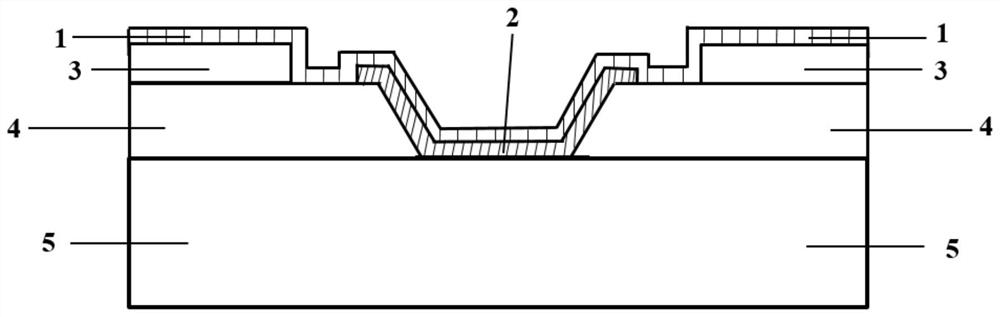
[0024] Such as figure 1 Shown, graphene / palladium selenide / silicon device of the present invention comprises graphene layer 1 successively from top to bottom, palladium diselenide layer 2, gold / indium electrode layer (or silver electrode layer) 3, silicon dioxide Insulation layer 4, n-type silicon substrate 5.

[0025] Further, the electrode 3 is a gold / indium alloy, wherein the gold electrode must be on the surface of the indium electrode layer, and the thickness of the gold layer is 50nm-150nm, and the thickness of the indium layer is 10nm-50nm, or directly replace it with a silver electrode with a thickness of 60nm-200nm .

[0026] Further, the area between the inner radius of the electrode and the n-type silicon round edge of the opening in...


PUM

PropertyMeasurementUnit
thicknessaaaaaaaaaa
thicknessaaaaaaaaaa
thicknessaaaaaaaaaa

Abstract

The invention discloses a graphene / palladium diselenide / silicon heterojunction self-driven photodetector, which is applied in the field of photoelectric detection technology. The existing photodetector is limited by the weak light absorption performance of graphene and has low responsivity. problem, the present invention first exposes the n-type silicon window by dry etching on the n-type silicon dioxide / silicon substrate; then coats a gold / indium electrode near the silicon window, and then adopts mechanical stripping to prepare a palladium diselenide microchip , and transfer palladium diselenide to the silicon window by positioning dry method; finally transfer graphene by wet transfer method, covering the surface of palladium diselenide and the electrode, wherein palladium diselenide is used as the interface between graphene and silicon A modification layer, a graphene layer corresponding to a single silicon window, a palladium diselenide layer, and an n-type silicon substrate form a graphene / palladium diselenide / silicon heterojunction; the device preparation process of the present invention is simple, and the device has self-driving , has excellent performance such as high responsivity in the visible-near-infrared light band.

Description

technical field [0001] The invention belongs to the technical field of photoelectric detection, and in particular relates to a self-driven photodetector and a preparation method thereof. Background technique [0002] Photodetectors are devices that convert optical signals into electrical signals. Although photodetectors made of traditional three-dimensional materials have good performance and mature manufacturing processes, they also have their shortcomings, such as infrared detectors. HgCdTe needs to work normally in a specific low temperature environment; photoresistors made of cadmium sulfide have a slow response time; silicon photodetectors have a relatively narrow detection bandwidth due to the limitation of silicon itself. Most importantly, detectors made of traditional three-dimensional materials are relatively difficult to integrate due to the severe surface states of three-dimensional materials. The emergence of two-dimensional materials can make up for some shortc...

Claims


Application Information

Patent Timeline
Patent Type & Authority Patents(China)
IPC IPC(8): H01L31/109H01L31/032H01L31/0352H01L31/18
CPCH01L31/109H01L31/032H01L31/035272H01L31/18Y02P70/50
Inventor 李永俊何天应兰长勇李春
Owner UNIV OF ELECTRONICS SCI & TECH OF CHINA
Why Eureka
Try Eureka