Light detection substrate and preparation method thereof, and light detection equipment

A technology for detecting substrates and light, which is applied in the field of photoelectric sensors, can solve the problems of MSM photoelectric characteristics damage, over-engraving, etc., and achieve the effect of improving photoelectric characteristics, avoiding oxidation, and avoiding film thinning

Active Publication Date: 2020-06-30
BOE TECH GRP CO LTD
View PDF5 Cites 4 Cited by
  • Summary
  • Abstract
  • Description
  • Claims
  • Application Information

AI Technical Summary

Problems solved by technology

[0004] The present invention aims at overlapping the opening position of the opening in the a-Si:H layer with the pattern of the MSM metal film layer below, resulting in over-etching of the MSM metal when the a-Si:H

Method used


Image

  • Light detection substrate and preparation method thereof, and light detection equipment
  • Light detection substrate and preparation method thereof, and light detection equipment
  • Light detection substrate and preparation method thereof, and light detection equipment

Examples


Embodiment Construction

[0037] In order to enable those skilled in the art to better understand the technical solution of the present invention, a light detection substrate, a manufacturing method thereof, and a light detection device of the present invention will be further described in detail below in conjunction with the accompanying drawings and specific embodiments.

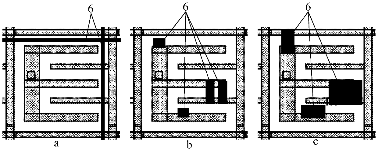
[0038] Metal-semiconductor-metal (Metal-Semiconductor-Metal, MSM) light detection structure has the advantages of fast response, small capacitance, simple process and easy integration, so it is widely used in the field of semiconductor detection, especially with various TFT backplanes Integrated as X-ray (X-ray) flat panel detector. Semiconductors in MSM light detectors usually use hydrogenated amorphous silicon a-Si:H. The active layer of the TFT used to output electrical signals in the TFT backplane usually uses a semiconductor metal oxide, such as IGZO.

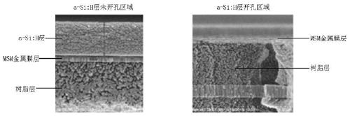
[0039]Due to the influence of the a-Si:H (hydrogenated amorphous silicon)...


PUM

PropertyMeasurementUnit
Thicknessaaaaaaaaaa
Thicknessaaaaaaaaaa
Slope angleaaaaaaaaaa

Abstract

The invention provides a light detection substrate and a preparation method thereof, and light detection equipment. The light detection substrate comprises a substrate and a plurality of light detection units arranged on the substrate, and the light detection units are arranged in an array; each light detection unit comprises a first electrode, a second electrode and a photoelectric conversion layer, wherein the photoelectric conversion layer is located on the sides, away from the substrate, of the first electrode and the second electrode, the orthographic projection of the photoelectric conversion layer on the substrate covers the first electrode and the second electrode, a spacing area is formed between the orthographic projections of the first electrode and the second electrode on the substrate, an opening is formed in the photoelectric conversion layer, and the orthographic projection of the opening on the substrate is located in the spacing area. According to the light detection substrate, the orthographic projection of the opening on the substrate is located in the interval area, namely the opening is formed in the non-overlapping area of the photoelectric conversion layer, the first electrode and the second electrode, and it can be ensured that the photoelectric characteristics of the light detection substrate are not damaged when patterns of the photoelectric conversionlayer and the opening are formed through etching.

Description

technical field [0001] The invention belongs to the technical field of photoelectric sensors, and in particular relates to a light detection substrate, a preparation method thereof, and light detection equipment. Background technique [0002] At present, metal-semiconductor-metal (Metal-Semiconductor-Metal, MSM) light detection structure has the advantages of fast response speed, small capacitance, simple process and easy integration, so it is widely used in the field of semiconductor detection, especially with various TFT The backplane is integrated into an X-ray (X-ray) flat panel detector. [0003] Semiconductors in MSM light detectors usually use hydrogenated amorphous silicon a-Si:H. The active layer of the TFT used to output electrical signals in the TFT backplane is usually made of amorphous silicon, but its mobility is low, only 0.5-1cm / V s, and semiconductor metal oxides, such as IGZO, can provide a larger The channel carrier mobility is as high as 10, so IGZO TFT...

Claims


Application Information

Patent Timeline
IPC IPC(8): H01L27/146H01L31/108
CPCH01L27/14643H01L27/14658H01L27/14683H01L31/1085H01L27/14607H01L27/14616H01L27/14692H01L27/14698H04N25/778
Inventor 孟凡理陈江博李凡梁魁李达张硕李泽源
Owner BOE TECH GRP CO LTD
Why Eureka
Try Eureka