Method for measuring p-layer carrier concentration of pin-type GaN avalanche device

A technology of carrier concentration and measurement method, which is applied in the field of detection of characteristic parameters of semiconductor optoelectronic devices, can solve problems such as unsuitability, large work function of gallium nitride materials, unsatisfactory performance, etc., and achieve the effect of reducing the difficulty of testing

Active Publication Date: 2020-07-03
INST OF SEMICONDUCTORS - CHINESE ACAD OF SCI
View PDF3 Cites 2 Cited by
  • Summary
  • Abstract
  • Description
  • Claims
  • Application Information

AI Technical Summary

Problems solved by technology

However, because the work function of the GaN material is very large, it is impossible to prepare an ohmic contact by finding a metal with a higher work function.
Generally, the ohmic contact made by tunneling effect is often not ideal, so it is not suitable for Hall test

Method used


Image

  • Method for measuring p-layer carrier concentration of pin-type GaN avalanche device
  • Method for measuring p-layer carrier concentration of pin-type GaN avalanche device
  • Method for measuring p-layer carrier concentration of pin-type GaN avalanche device

Examples


Embodiment Construction

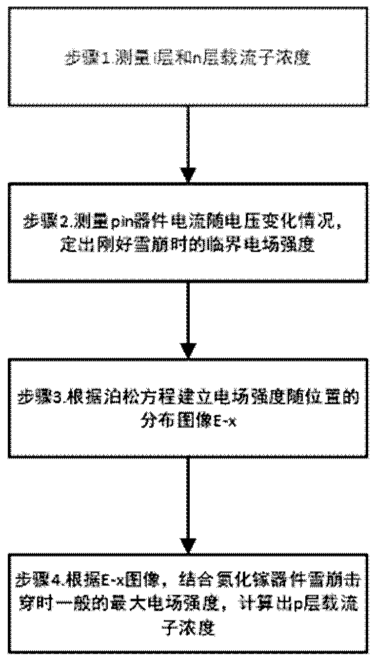
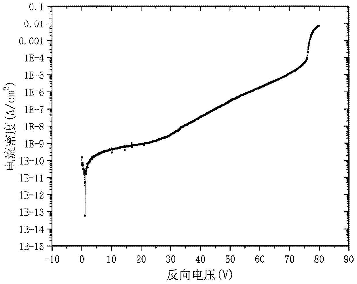
[0028] The invention discloses a method for obtaining the p-layer carrier concentration of a pin-type GaN avalanche device. The basis of this method is that the critical avalanche breakdown voltage can be measured by the probe test platform, the carrier concentration will affect the electric field intensity distribution of the device, and the integral sum of the electric field intensity with the position is the critical avalanche voltage. Combining the measured i-layer concentration, n-layer concentration, p-layer thickness, i-layer thickness, and the maximum electric field strength when gallium nitride just breaks down, the p-layer carrier concentration can be solved by listing the equation.

[0029] Specifically, such as figure 1 As shown, the steps of obtaining the p-layer carrier concentration in the present invention are as follows:

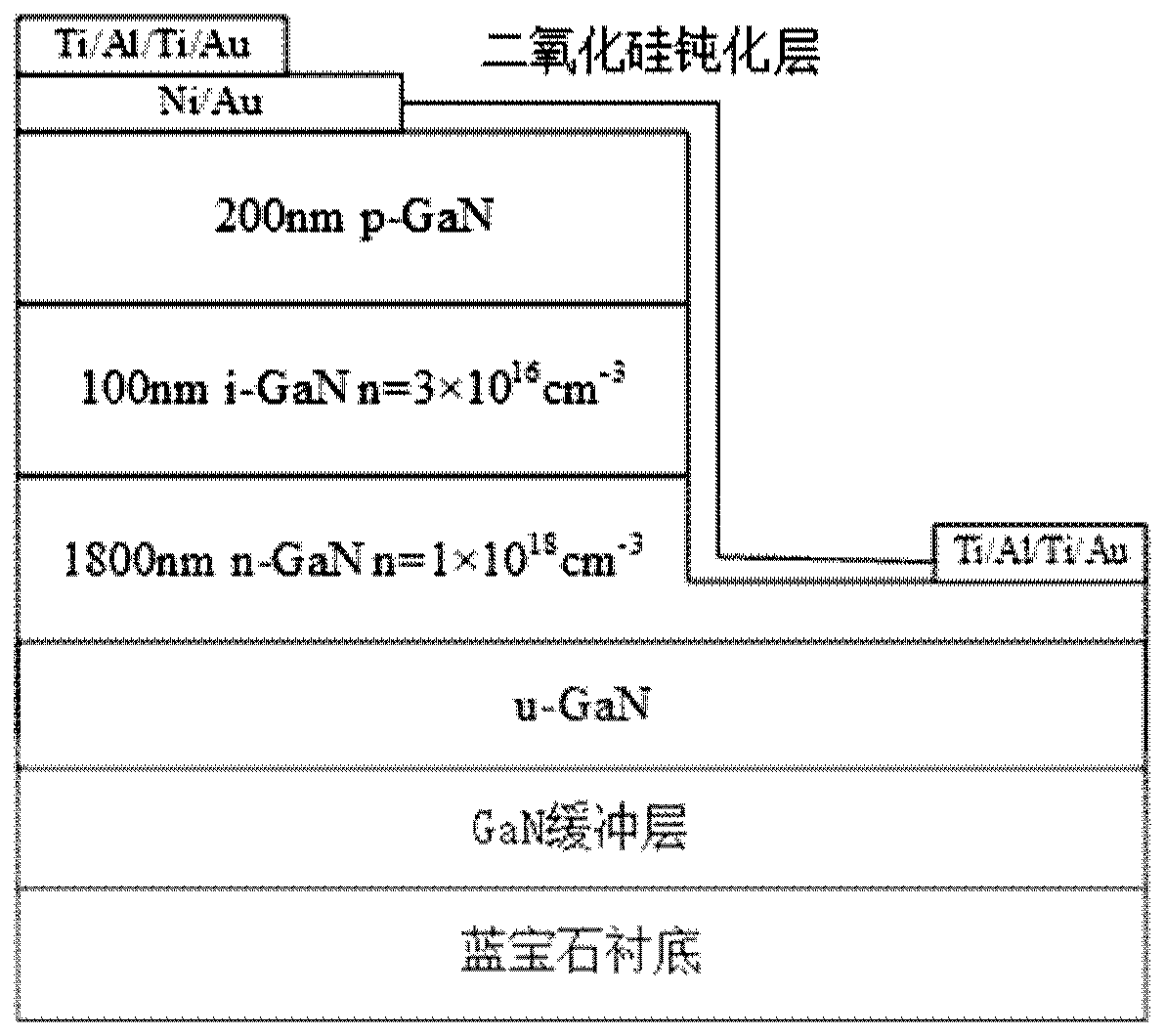
[0030] Step 1. First, a single-layer i-layer and n-layer gallium nitride sample is grown by metal organic compound chemical vapor depositi...


PUM

PropertyMeasurementUnit
relative permittivityaaaaaaaaaa

Abstract

The invention discloses a method for measuring the p-layer carrier concentration of a GaN avalanche detector, which comprises the steps of growing an i-layer gallium nitride and an n-layer gallium nitride in a distributed manner under the same condition, performing ohmic contact by using a metal electrode, and testing the carrier concentration of the corresponding i-layer and n-layer by using a Hall effect; obtaining a current-voltage curve of the pin-type GaN avalanche detector device during reverse bias under the condition of no illumination, and reading a critical reverse voltage value whenthe current just begins to be exponentially increased; establishing an electric field intensity distribution diagram E-x of the pin-type GaN avalanche detector device under reverse bias according toa Poisson equation; and according to the maximum electric field intensity when the gallium nitride material is just subjected to avalanche breakdown, reversely deducing the p-layer carrier concentration according to the measured critical reverse voltage value in combination with an electric field intensity distribution diagram. The test method disclosed by the invention is a non-consumable test method, and can be used for repeatedly detecting the sample.

Description

technical field [0001] The invention relates to the technical field of detection of characteristic parameters of semiconductor photoelectric devices, in particular to a method for measuring the carrier concentration of a p-layer of a pin-type GaN avalanche device. Background technique [0002] Migrating electrons or holes in semiconductors, that is, carriers, are the core carriers of optoelectronic devices. Carriers are continuously generated and recombined in the device, and their concentration can affect the impact ionization and other phenomena in the avalanche device, thus playing a key role in the breakdown voltage and multiplication factor of the avalanche device. In view of this, the carrier concentration of an avalanche detector is the core information that determines the device performance. [0003] The general method of measuring the carrier concentration of a certain layer is to make an ohmic contact on a single-layer sample, and then use the Hall test to measure...

Claims


Application Information

Patent Timeline
Patent Type & Authority Applications(China)
IPC IPC(8): G01R31/26
CPCG01R31/2601
Inventor 曹子坤赵德刚梁锋杨静朱建军刘宗顺
Owner INST OF SEMICONDUCTORS - CHINESE ACAD OF SCI
Why Eureka
Try Eureka