Test probe, optical chip module test probe assembly, probe assembly assembling method and optical chip module test device

A test probe and module testing technology, which is applied to measurement devices, measurement device housings, and electronic circuit testing, etc. The size of the test probe should not be too large to achieve the effect of reducing the overall processing and assembly difficulty, improving reliability and stability, and avoiding errors

Pending Publication Date: 2020-07-10
SUZHOU CHUANGRUI MACHINERY & ELECTRICAL TECH
View PDF3 Cites 2 Cited by
  • Summary
  • Abstract
  • Description
  • Claims
  • Application Information

AI Technical Summary

Problems solved by technology

[0003] In the process of COM / QFP optical chip module processing, chip performance testing needs to be carried out through special test fixtures. During the test, the electrical connection is realized by contacting the test probes with the pins of the chip module. Currently, the tubes of the chip module The diameter of the pin is basically within 0.05mm, and even the pins of many chips are within 0.03mm. At the same time, because the distance between the pins is about 0.2mm, the size of the test probe itself should not be too large. A test probe, usually in order to make it have a certain stretchability to avoid hard contact, the test probe is integrated with elastic parts such as springs, such as the test probes disclosed in the application numbers 201780069227.3 and 201080067768.0, which causes the test probe The structure of the needle is complex and the size is large
[0004] There are also some test probes that use straight or polygonal special-shaped rhenium-tungsten needles, and their test ends are usually set in the shape of a ball or needle as shown in the above patent, which results in a short contact area between the test probe and the chip pin. , it is required that the tolerance range between the test probe and the chip pin or PAD is about 0.02mm to be in effective contact. However, due to the existence of various processing and assembly tolerances, it is easy to appear that the test probe and the chip pin cannot be effectively contacted. contact, resulting in a higher probability of an open circuit
[0005] There are also other probes that are shaped shrapnel, which are prone to deformation during use, resulting in inaccurate positioning
[0006] At the same time, the existing test probe structure greatly improves the processing and assembly accuracy requirements of other structures, which increases the difficulty of processing and assembly

Method used


Image

  • Test probe, optical chip module test probe assembly, probe assembly assembling method and optical chip module test device
  • Test probe, optical chip module test probe assembly, probe assembly assembling method and optical chip module test device
  • Test probe, optical chip module test probe assembly, probe assembly assembling method and optical chip module test device

Examples


Embodiment Construction

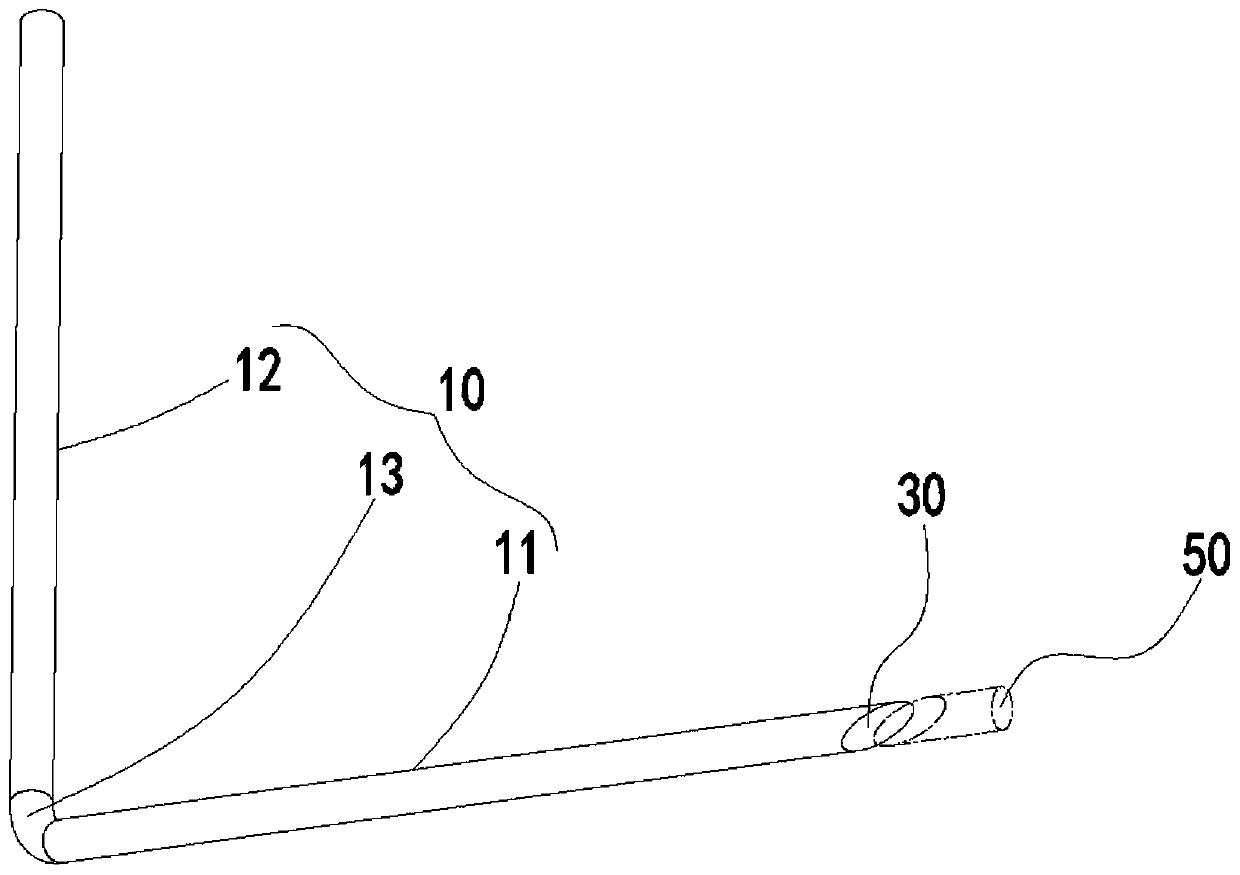
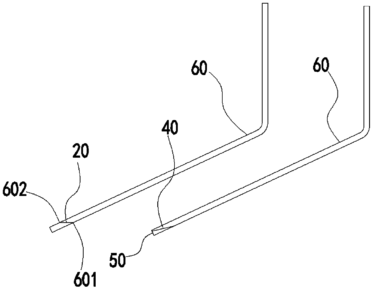
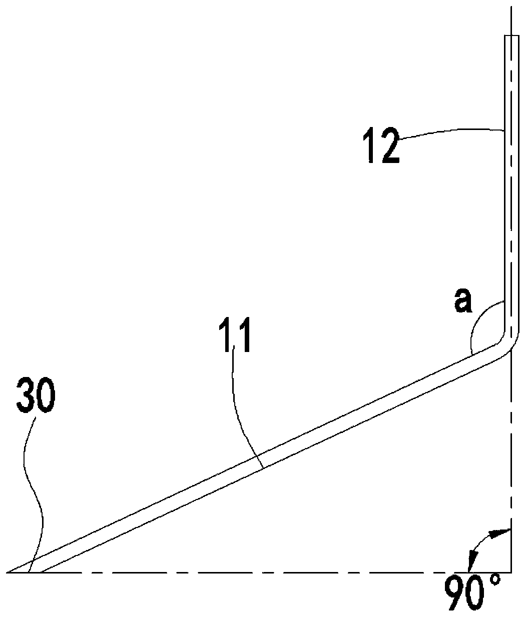
[0056] Objects, advantages and features of the present invention will be illustrated and explained by the following non-limiting description of preferred embodiments. These embodiments are only typical examples of applying the technical solutions of the present invention, and all technical solutions formed by adopting equivalent replacements or equivalent transformations fall within the protection scope of the present invention.

[0057] In the description of the scheme, it should be noted that the terms "center", "upper", "lower", "left", "right", "front", "rear", "vertical", "horizontal", " The orientation or positional relationship indicated by "inner", "outer", etc. is based on the orientation or positional relationship shown in the drawings, and is only for the convenience of description and simplification of description, rather than indicating or implying that the device or element referred to must have a specific orientation , constructed and operated in a particular or...


PUM

PropertyMeasurementUnit
diameteraaaaaaaaaa

Abstract

The invention discloses a test probe, an optical chip module test probe assembly, a probe assembly assembling method and an optical chip module test device. The test probe comprises a probe main body,the test end of the probe main body is beveled to form a beveled plane, and the area of the beveled plane is larger than that of the end face of the test end before cutting. According to the scheme,the structure is simple, the test probe does not need structures such as a spring, size is greatly reduced, the use requirement of the small tube foot step pitch can be met, and the area of the beveled plane is larger than that of the end face of the probe body before cutting. Compared with the probes in the prior art, the contact area can be effectively increased, the position tolerance range between the test probe and the pin is widened, and the overall processing and assembling difficulty of the test equipment is reduced, the open circuit condition can be reduced under the condition of conventional processing and assembling precision and the test reliability and stability are improved.

Description

technical field [0001] The invention relates to the field of chip test equipment, in particular to a test probe, an optical chip module test probe assembly, a probe assembly assembly method and an optical chip module test device. Background technique [0002] COM / QFP optical chip module is a module composed of a photosensitive chip and a related frame structure that emerged with circuit integration and optical integration. The circuit signal is exported using tinned copper wire or gold wire, etc. And the design of the step distance between tinned copper wire / gold wire is getting smaller and smaller, and it has reached about 0.2mm at present. [0003] In the process of COM / QFP optical chip module processing, chip performance testing needs to be carried out through special test fixtures. During the test, the electrical connection is realized by contacting the test probes with the pins of the chip module. Currently, the tubes of the chip module The diameter of the pin is basic...

Claims


Application Information

Patent Timeline
Patent Type & Authority Applications(China)
IPC IPC(8): G01R31/28G01R1/067G01R1/04G01R3/00
CPCG01R1/0408G01R1/06738G01R1/06755G01R3/00G01R31/2851
Inventor 朱小刚
Owner SUZHOU CHUANGRUI MACHINERY & ELECTRICAL TECH
Why Eureka
Try Eureka